
Processor Users Manual

10-16 MPC8260 PowerQUICC II UserÕs Manual MOTOROLA
Part III. The Hardware Interface
10.3.2 Option Registers (ORx)
The ORx registers deÞne the sizes of memory banks and access attributes. The ORx
attributes bits support the following three modes of operation as deÞned by BR[MS].
¥ SDRAM mode
¥ GPCM mode
¥ UPM mode
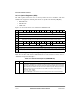
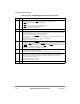
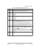
Figure 10-7 shows the ORx as it is formatted for SDRAM mode.
Table 10-4 describes ORx Þelds in SDRAM mode. For more details see Section 10.4.12,
ÒSDRAM ConÞguration Examples.Ó
Bit 0 1 2 3 4 5 6 7 8 9 10 11 12 13 14 15
Field SDAM LSDAM...
Reset 0000_0000_0000_0000
R/W R/W
Addr 0x10104 (OR0); 0x1010C (OR1); 0x10114 (OR2); 0x1011C (OR3); 0x10124 (OR4); 0x1012C (OR5); 0x10134
(OR6); 0x1013C (OR7); 0x10144 (OR8); 0x1014C (OR9); 0x10154 (OR10); 0x1015C (OR11)
Bit 16 17 18 19 20 21 22 23 24 25 26 27 28 29 30 31
Field ...LSDAM BPD ROWST Ñ NUMR PMSEL IBID Ñ
Reset 0000_0000_0000_0000
R/W R/W
Addr 0x10106 (OR0); 0x1010E (OR1); 0x10116 (OR2); 0x1011E (OR3); 0x10126 (OR4); 0x1012E (OR5); 0x10136
(OR6); 0x1013E (OR7); 0x10146 (OR8); 0x1014E (OR9); 0x10156 (OR10); 0x1015E (OR11)
Figure 10-7. Option Registers (ORx)ÑSDRAM Mode
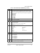
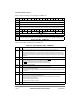
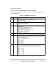
Table 10-4. ORx Field Descriptions (SDRAM Mode)
Bits Name Description
0Ð4 SDAM SDRAM address mask. Provides masking for corresponding BRx bits. By masking address bits
independently, SDRAM devices of different size address ranges can be used. Clearing bits masks
the corresponding address bit. Setting bits causes the corresponding address bit to be compared
with the address pins. Address mask bits can be set or cleared in any order, allowing a resource to
reside in more than one area of the address map. SDAM can be read or written at any time.
0000_0000_0000 = 4Gbyte
1111_1111_1111 = 1 Mbyte
Note: if xSDMR[PBI]=0, the maximum size of the memory bank should not exceed 128 Mbytes.