
Processor Users Manual

10-18 MPC8260 PowerQUICC II UserÕs Manual MOTOROLA
Part III. The Hardware Interface
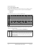
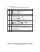
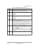
Figure 10-8 shows ORx as it is formatted for GPCM mode.
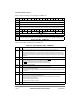
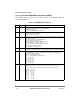
Table 10-5 describes ORx Þelds in GPCM mode.
27 IBID Internal bank interleaving within same device disable. Setting this bit disables bank interleaving
between internal banks of a SDRAM device connected to the chip-select line. IBID should be set
in 60x-compatible mode if the SDRAM device is not connected to the BANKSEL pins.
28Ð31 Ñ Reserved, should be cleared.
Bit 0 1 2 3 4 5 6 7 8 9 10 11 12 13 14 15
Field AM...
Reset 1111_1110_0000_0000
R/W R/W
Addr 0x10104 (OR0); 0x1010C (OR1); 0x10114 (OR2); 0x1011C (OR3); 0x10124 (OR4); 0x1012C (OR5);
0x10134 (OR6); 0x1013C (OR7); 0x10144 (OR8); 0x1014C (OR9); 0x10154 (OR10); 0x1015C (OR11)
Bit 16 17 18 19 20 21 22 23 24 25 26 27 28 29 30 31
Field ...AM Ñ BCTLD CSNT ACS Ñ SCY SETA TRLX EHTR Ñ
Reset 0 00 0
1 11 0 1111 0 1 0 0
R/W R/W
Addr 0x10106 (OR0); 0x1010E (OR1); 0x10116 (OR2); 0x1011E (OR3); 0x10126 (OR4); 0x1012E (OR5); 0x10136
(OR6); 0x1013E (OR7); 0x10146 (OR8); 0x1014E (OR9); 0x10156 (OR10); 0x1015E (OR11)
Figure 10-8. ORx ÑGPCM Mode
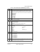
Table 10-5. ORxÑGPCM Mode Field Descriptions
Bits Name Description
0Ð16 AM Address mask. Masks corresponding BRx bits. Masking address bits independently allows external
devices of different size address ranges to be used.
0 Corresponding address bits are masked.
1 The corresponding address bits are used in the comparison with address pins. Address mask bits
can be set or cleared in any order in the Þeld, allowing a resource to reside in more than one area
of the address map. AM can be read or written at any time.
Note: After system reset, OR0[AM] is 1111_1110_0000_0000_0.
17Ð18 Ñ Reserved, should be cleared.
19 BCTLD Data buffer control disable. Disables the assertion of BCTL
x during access to the current memory
bank. See Section 10.2.7, ÒData Buffer Controls (BCTLx).Ó
0 BCTLx
is asserted upon access to the current memory bank.
1 BCTLx
is not asserted upon access to the current memory bank.
20 CSNT Chip-select negation time. Determines when CS
/WE are negated during an external memory write
access handled by the GPCM. This helps meet address/data hold times for slow memories and
peripherals.
0CS
/WE are negated normally.
1CS
/WE are negated a quarter of a clock earlier.
Note: After system reset OR0[CSNT] is set.
Table 10-4. ORx Field Descriptions (SDRAM Mode) (Continued)
Bits Name Description