
Processor Users Manual

MOTOROLA Chapter 10. Memory Controller 10-21
Part III. The Hardware Interface
10.3.3 60x SDRAM Mode Register (PSDMR)
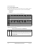
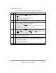
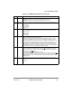
The 60x SDRAM mode register (PSDMR), shown in Figure 10-10, is used to conÞgure
operations pertaining to SDRAM.
Table 10-7 describes PSMDR Þelds. LSMDR Þelds are described in Table 10-8.
Bit 0 1 2 3 4 5 6 7 8 9 10 11 12 13 14 15
Field PBI RFEN OP SDAM BSMA SDA10 RFRC
Reset 0000_0000_0000_0000
R/W R/W
Addr 0x10190 (PSDMR), 0x10194 (LSDMR)
Bit 16 17 18 19 20 21 22 23 24 25 26 27 28 29 30 31
Field RFRC PRETOACT ACTTORW BL LDOTOPRE WRC EAMUX BUFCMD
CL
Reset 0000_0000_0000_0000
R/W R/W
Addr 0x10192 (PSDMR), 0x10196 (LSDMR)
Figure 10-10. 60x/Local SDRAM Mode Register (PSDMR/LSDMR)
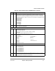
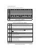
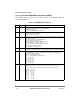
Table 10-7. PSDMR Field Descriptions
Bits Name Description
0 PBI Page-based interleaving. Selects the address multiplexing method. PBI works in conjunction
with ORx[SDA10]. See Section 10.4.5, ÒBank Interleaving.Ó
0 Bank-based interleaving
1 Page-based interleaving (normal operation)
1 RFEN Refresh enable. Indicates that the UPM needs refresh services.
0 Refresh services are not required
1 Refresh services are required
Note: After system reset, RFEN is cleared.
See Section 10.3.8, Ò60x Bus-Assigned UPM Refresh Timer (PURT),Ó Section 10.3.9, ÒLocal
Bus-Assigned UPM Refresh Timer (LURT),Ó Section 10.3.10, Ò60x Bus-Assigned SDRAM
Refresh Timer (PSRT),Ó and Section 10.3.11, ÒLocal Bus-Assigned SDRAM Refresh Timer
(LSRT).Ó
2Ð4 OP SDRAM operation. Determines which operation occurs when the SDRAM device is accessed.
000 Normal operation
001 CBR refresh, used in SDRAM initialization.
010 Self refresh (for debug purpose).
011 Mode Register write, used in SDRAM initialization.
Note that if 60x-compatible mode is in effect on the 60x bus, the bus master must supply the
mode register data on the low bits of the address during the access.
100 Precharge bank (for debug purpose).
101 Precharge all banks, used in SDRAM initialization.
110 Activate bank (for debug purpose).
111 Read/write (for debug purpose).
5Ð7 SDAM Address multiplex size. Determines how the address of the current memory cycle can be output
on the address pins. See Section 10.4.5.1, ÒSDRAM Address Multiplexing (SDAM and BSMA).Ó