
Processor Users Manual

10-26 MPC8260 PowerQUICC II UserÕs Manual MOTOROLA
Part III. The Hardware Interface
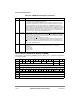
10.3.5 Machine A/B/C Mode Registers (MxMR)
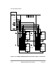
The machine x mode registers (MxMR), shown in Figure 10-11, contain the conÞguration
for the three UPMs.
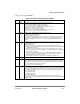
28 EAMUX External address multiplexing enable/disable.
0 No external address multiplexing. Fastest timing.
1 The memory controller asserts SDAMUX for an extra cycle before issuing an
ACTIVATE
command to the SDRAM. This is useful when external address multiplexing can cause a
delay on the address lines. Note that if EAMUX is set, ACTTORW should be at least 2.
In 60x-compatible mode, external address multiplexing is placed on the address lines. If the
additional delay of the multiplexing endangers the device setup time, EAMUX should be set.
Setting this bit causes the memory controller to add another cycle for each address phase.
Note that EAMUX can also be set in case of address line delays, such as address buffers.
See Section 10.4.6.7, ÒExternal Address Multiplexing Signal.Ó
29 BUFCMD If external buffers are placed on the control lines going to both the SDRAM and address lines,
setting BUFCMD causes all SDRAM control lines except CS
to be asserted for two cycles,
instead of one. See Section 10.4.6.8, ÒExternal Address and Command Buffers (BUFCMD).Ó
0 Normal timing for the control lines
1 All control lines except CS
are asserted for two cycles
In 60x-compatible mode, external buffers may be placed on the command strobes, except
CS
, as well as the address lines. If the additional delay of the buffers is endangering the
device setup time, BUFCMD should be set to cause the memory controller to add another
cycle for each SDRAM command.
30Ð31 CL CAS latency. DeÞnes the timing for Þrst read data after a column address is sampled by the
SDRAM. See Section 10.4.6.3, ÒColumn Address to First Data OutÑCAS Latency.Ó
00 Reserved
01 1 clock cycle
10 2 clock cycles
11 3 clock cycles
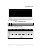
Bit 0 1 2 3 4 5 6 7 8 9 10 11 12 13 14 15
Field BSEL RFEN OP Ñ AMx DSx G0CLx GPL_x4DIS RLFx
Reset 0000_0000_0000_0
100
R/W R/W
Addr 0x10170 (MAMR); 0x10174 (MBMR); 0x10178 (MCMR)
Bit 16 17 18 19 20 21 22 23 24 25 26 27 28 29 30 31
Field RLFx WLFx TLFx MAD
Reset 0000_0000_0000_0000
R/W R/W
Addr 0x10172 (MAMR); 0x10176 (MBMR); 0x1017A (MCMR)
Figure 10-11. Machine x Mode Registers (MxMR)
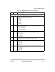
Table 10-8. LSDMR Field Descriptions (Continued)
Bits Name Description