
Processor Users Manual

10-28 MPC8260 PowerQUICC II UserÕs Manual MOTOROLA
Part III. The Hardware Interface
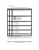
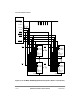
10.3.6 Memory Data Register (MDR)
The memory data register (MDR), shown in Figure 10-12, contains data written to or read
from the RAM array for UPM
READ or WRITE commands. MDR must be set up before
issuing a write command to the UPM.
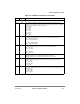
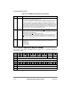
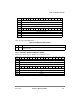
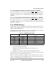
10Ð12 G0CLx General line 0 control. Determines which address line can be output to the GPL0 pin when the
UPMx is selected to control the memory access.
000 A12
001 A11
010 A10
011 A9
100 A8
101 A7
110 A6
111 A5
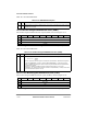
13 GPL_x4DIS GPL_A4 output line disable. Determines if the UPWAIT/GT
A/GPL_4 pin behaves as an output
line controlled by the corresponding bits in the UPMx array (GPL4x).
0 UPWAIT/GT
A/GPL_x4 behaves as GPL_4.
UPMx[G4T4/DLT3] is interpreted as G4T4.
The UPMx[G4T3/WAEN] is interpreted as G4T3.
1 UPWAIT/GT
A/GPL_x4 behaves as UPWAIT.
UPMx[G4T4/DLT3] is interpreted as DLT3.
UPMx[G4T3/WAEN] is interpreted as WAEN.
Note: After a system reset, GPL_x4DIS = 1.
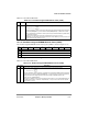
14Ð17 RLFx Read loop Þeld. Determines the number of times a loop deÞned in the UPMx will be executed
for a burst- or single-beat read pattern or when MxMR[OP] = 11 (
RUN command)
0001 The loop is executed 1 time
0010 The loop is executed 2 times
...
1111 The loop is executed 15 times
0000 The loop is executed 16 times
18Ð21 WLFx Write loop Þeld. Determines the number of times a loop deÞned in the UPMx will be executed for
a burst- or single-beat write pattern.
0001 The loop is executed 1 time
0010 The loop is executed 2 times
...
1111 The loop is executed 15 times
0000 The loop is executed 16 times
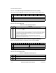
22Ð25 TLFx Refresh loop Þeld. Determines the number of times a loop deÞned in the UPMx will be executed
for a refresh service pattern.
0001 The loop is executed 1 time
0010 The loop is executed 2 times
...
1111 The loop is executed 15 times
0000 The loop is executed 16 times
26Ð31 MAD Machine address. RAM address pointer for the command executed. This Þeld is incremented by
1, each time the UPM is accessed and the OP Þeld is set to WRITE or READ.
Table 10-9. Machine x Mode Registers (MxMR) (Continued)
Bits Name Description