
Processor Users Manual

MOTOROLA Chapter 10. Memory Controller 10-29
Part III. The Hardware Interface
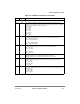
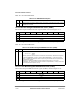
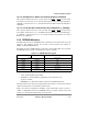
Table 10-10 describes MDR Þelds.
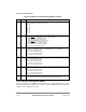
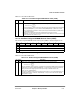
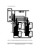
10.3.7 Memory Address Register (MAR)
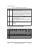
The memory address register (MAR) is shown in Figure 10-13.
Bit 0 1 2 3 4 5 6 7 8 9 10 11 12 13 14 15
Field MD
Reset 0000_0000_0000_0000
R/W R/W
Addr 0x10188
Bit 16 17 18 19 20 21 22 23 24 25 26 27 28 29 30 31
Field MD
Reset 0000_0000_0000_0000
R/W R/W
Addr 0x1018A
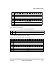
Figure 10-12. Memory Data Register (MDR)
Table 10-10. MDR Field Descriptions
Bits Name Description
0Ð31 MD Memory data. The data to be read or written into the RAM array when a
WRITE or READ command is
supplied to the UPM.
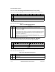
Bit 0 1 2 3 4 5 6 7 8 9 10 11 12 13 14 15
Field A
Reset 0000_0000_0000_0000
R/W R/W
Addr 0x10168
Bit 16 17 18 19 20 21 22 23 24 25 26 27 28 29 30 31
Field A
Reset 0000_0000_0000_0000
R/W R/W
Addr 0x10116A
Figure 10-13. Memory Address Register (MAR)