
Processor Users Manual

MOTOROLA Chapter 10. Memory Controller 10-49
Part III. The Hardware Interface
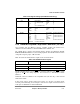
Now, from the SDRAM device point of view, during an ACTIVATE command, its address
port should look like Table 10-22
.
Table 10-19 indicates that to multiplex A[6Ð17] over A[17Ð28], PSDMR[SDAM] must be
011 and, because the internal bank selects are multiplexed over A[15Ð16], PSDMR[BSMA]
must be 010 (only the lower two bank select lines are used).
Note that if the device is connected to the BNKSEL pins, the value of PSDMR[BSMA] has
no effect. In the above example, address lines [18Ð19] are output on BNKSEL1 and
BNKSEL0, accordingly.
During a
READ/WRITE command, the address port should look like Table 10-23.
Because AP alternates with A[7] of the row lines, set PSDMR[SDA10] = 011. This outputs
A[7] on the SDA10 line during the
ACTIVATE command and AP during READ/WRITE and
CBR commands.
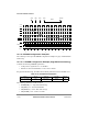
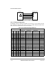
Table 10-24 shows the register conÞguration. Not shown are PSRT and MPTPR, which
should be programmed according to the device refresh requirements:
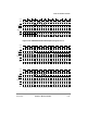
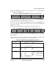
Table 10-22. SDRAM Device Address Port during ACTIVATE Command
ÒA[0Ð14]Ó A[15Ð16] A[17Ð28] A[29Ð31]
Ñ Internal bank select (A[18Ð19]) Row (A[6Ð17]) n.c.
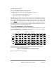
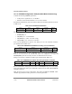
Table 10-23. SDRAM Device Address Port during READ/WRITE Command
ÒA[0Ð14]Ó A[15Ð16] A[17] A[18] A[19] A[20Ð28] A[29Ð31]
Ñ Internal bank select DonÕt care AP DonÕt care Column n.c.
Table 10-24. Register Settings (Page-Based Interleaving
Register Settings
BRx BA Base address
PS 00 = 64-bit port size
DECC 00
WP 0
MS 010 = SDRAM-60x bus
EMEMC 0
ATOM 00
DR 0
V1
ORx AM 1111_1100_0000
LSDAM 00000
BPD 01
ROWST 0110
NUMR 011
PMSEL 0
IBID 0
PSDMR PBI 1
RFEN 1
OP 000
SDAM 011
BSMA 010
SDA10 011
RFRC from device data sheet
PRETOACT from device data sheet
ACTTOROW from device data sheet
BL 0
LDOTOPRE from device data sheet
WRC from device data sheet
EAMUX 0
BUFCMD 0
CL from device data sheet