
Processor Users Manual

10-50 MPC8260 PowerQUICC II UserÕs Manual MOTOROLA
Part III. The Hardware Interface
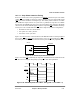
10.4.13 SDRAM ConÞguration Example (Bank-Based Interleaving)
Consider the following SDRAM organization:
¥ 64-bit port size organized as 8 x 8 x 64 Mbit.
¥ Each device has four internal banks, 12 rows, and 9 columns
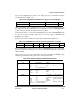
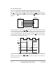
For bank-based Interleaving, this means that the address bus should be partitioned as shown
in Table 10-25.
The following parameters can be extracted:
¥ PSDMR[PBI] = 0
¥ORx[BPD] = 01Ñ4 internal banks
¥ORx[ROWST] = 0100Ñrow starts at A[8]
¥ORx[NUMR] = 011Ñthere are 12 row lines
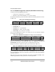
Now, from the SDRAM device point of view, during an
ACTIVATE command, its address
port should look like Table 10-26
.
Table 10-19 indicates that in order to multiplex A[6Ð19] over A[15Ð28] PSDMR[SDAM]
must be 001 and, because the internal bank selects are multiplexed over A[15Ð16]
PSDMR[BSMA] must be 010 (only the lower two bank select lines are used).
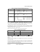
During a
READ/WRITE command, the address port should look like Table 10-27.
Because AP alternates with A[9] of the row lines, set PSDMR[SDA10] = 011. This outputs
A[9] on the SDA10 line during the ACTIVATE command and AP during READ/WRITE
and CBR commands.
Table 10-28 shows the register conÞguration. Not shown are PSRT and MPTPR, which
should be programmed according to the device refresh requirements.
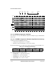
Table 10-25. 60x Address Bus Partition
A[0Ð5] A[6Ð7] A[8Ð19] A[20Ð28] A[29Ð31]
msb of start address Internal bank select Row Column lsb
Table 10-26. SDRAM Device Address Port during ACTIVATE Command
ÒA[0Ð14]Ó A[15Ð16] A[17Ð28] A[29Ð31]
Ñ Internal bank select (A[6Ð7]) Row (A[8Ð19]) n.c.
Table 10-27. SDRAM Device Address Port during READ/WRITE Command
ÒA[0Ð14]Ó A[15Ð16] A[17] A[18] A[19] A[20Ð28] A[29Ð31]
Ñ Internal bank select DonÕt care AP DonÕt care Column n.c.