
Processor Users Manual

MOTOROLA Chapter 10. Memory Controller 10-51
Part III. The Hardware Interface
10.5 General-Purpose Chip-Select Machine (GPCM)
Users familiar with the MPC8xx memory controller should read Section 10.5.4,
ÒDifferences between MPC8xxÕs GPCM and MPC8260Õs GPCM,Ó Þrst.
The GPCM allows a glueless and ßexible interface between the MPC8260, SRAM,
EPROM, FEPROM, ROM devices, and external peripherals. The GPCM contains two basic
conÞguration register groupsÑBRx and ORx.
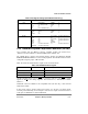
Table 10-29 lists the GPCM interface signals on the 60x and local bus.
GPCM-controlled devices can use BCTL
x as read/write indicators. The BCTLx signals
appears as R/W
in the timing diagrams. See Section 10.2.7, ÒData Buffer Controls
(BCTLx).Ó
Additional control is available in 60x-compatible mode (60x bus only)ÑALEÐexternal
address latch enable
In this section, when a signal is named, the reference is to the 60x or local bus signal,
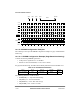
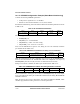
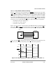
according to the bank being accessed. Figure 10-40 shows a simple connection between a
32-bit port size SRAM device and the MPC8260.
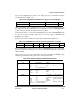
Table 10-28. Register Settings (Bank-Based Interleaving)
Register Settings
BRx BA Base address
PS 00 = 64-bit port size
DECC 00
WP 0
MS 010 = SDRAM-60x bus
EMEMC 0
ATOM 00
DR 0
V1
ORx SDAM 1111_1100_0000
LSDAM 00000
BPD 01
ROWST 010
NUMR 011
PMSEL 0
IBID 0
PSDMR PBI 0
RFEN 1
OP 000
SDAM 001
BSMA 010
SDA10 011
RFRC from device data sheet
PRETOACT from device data sheet
ACTTOROW from device data sheet
BL 0
LDOTOPRE from device data sheet
WRC from device data sheet
EAMUX 0
BUFCMD 0
CL from device data sheet
Table 10-29. GPCM Interfaces Signals
60x Bus Local Bus Comments
CS[0Ð11]
Device select
WE[0Ð7]
LWE[0Ð3] Write enables for write cycles
OE
LOE Output enable for read cycles