
Processor Users Manual

MOTOROLA Chapter 10. Memory Controller 10-59
Part III. The Hardware Interface
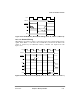
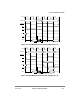
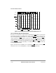
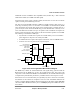
Figure 10-51. GPCM Read Followed by Read (ORx[29Ð30] = 01)
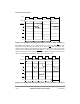
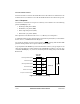
Figure 10-52. GPCM Read Followed by Write (ORx[29Ð30] = 01)
Clock
Address
PSD
VAL
CSx
CSy
R/W
OE
Data
Hold Time 1-cycle hold time allowed
Clock
Address
PSD
VAL
CSx
CSy
R/W
OE
Data
Hold Time Long hold time allowed