
Processor Users Manual

10-72 MPC8260 PowerQUICC II UserÕs Manual MOTOROLA
Part III. The Hardware Interface
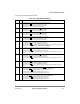
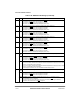
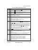
12 G1T1 General-purpose line 1 timing 1. DeÞnes the state of GPL1 during phase 1Ð2.
0 The value of the GPL0
line at the rising edge of T1 will be 0
1 The value of the GPL0
line at the rising edge of T1 will be 1
See Section 10.6.4.1.3, ÒGeneral-Purpose Signals (GxTx, GOx).Ó
13 G1T3 General-purpose line 1 timing 3. DeÞnes the state of GPL1
during phase 3Ð4.
0 The value of the GPL1
line at the rising edge of T3 will be 0
1 The value of the GPL1
line at the rising edge of T3 will be 1
See Section 10.6.4.1.3, ÒGeneral-Purpose Signals (GxTx, GOx).Ó
14 G2T1 General-purpose line 2 timing 1. DeÞnes the state of GPL2
during phase 1Ð2.
0 The value of the GPL2
line at the rising edge of T1 will be 0
1 The value of the GPL2
line at the rising edge of T1 will be 1
See Section 10.6.4.1.3, ÒGeneral-Purpose Signals (GxTx, GOx).Ó
15 G2T3 General-purpose line 2 timing 3. DeÞnes the state of GPL2
during phase 3Ð4.
0 The value of the GPL2
line at the rising edge of T3 will be 0
1 The value of the GPL2
line at the rising edge of T3 will be 1
See Section 10.6.4.1.3, ÒGeneral-Purpose Signals (GxTx, GOx).Ó
16 G3T1 General-purpose line 3 timing 1. DeÞnes the state of GPL3
during phase 1Ð2.
0 The value of the GPL3
line at the rising edge of T1 will be 0
1The value of the GPL3
line at the rising edge of T1 will be 1
See Section 10.6.4.1.3, ÒGeneral-Purpose Signals (GxTx, GOx).Ó
17 G3T3 General-purpose line 3 timing 3. DeÞnes the state of GPL3
during phase 3Ð4.
0 The value of the GPL3
line at the rising edge of T3 will be 0
1 The value of the GPL3
line at the rising edge of T3 will be 1
See Section 10.6.4.1.3, ÒGeneral-Purpose Signals (GxTx, GOx).Ó
18 G4T/
DLT2
General-purpose line 4 timing 1/delay time 2. The function is determined by MxMR[GPLx4DIS].
G4T1 If MxMR deÞnes UPWAITx/GPL_x4
as an output (GPL_x4), this bit functions as G4T1:
0 The value of the GPL4
line at the rising edge of T1 will be 0
1 The value of the GPL4
line at the rising edge of T1 will be 1
See Section 10.6.4.1.3, ÒGeneral-Purpose Signals (GxTx, GOx).Ó
DLT3 If MxMR[GPLx4DIS] = 1, UPWAITx is chosen and this bit functions as DLT3.
0 In the current word, indicates that the data bus should be sampled at the rising edge of T1 (if a read
burst or a single read service is executed).
1 In the current word, indicates that the data bus should be sampled at the rising edge of T3 (if a read
burst or a single read service is executed).
For an example, see Section 10.6.4.3, ÒData Valid and Data Sample Control.Ó
19 G4T3/
W
AEN
General-purpose line 4 timing 3/wait enable. Function depends on the value of MxMR[GPLx4DIS].
G4T3 If MxMR[GPLx4DIS] = 0, G4T3 is selected.
0 The value of the GPL4
line at the rising edge of T3 will be 0
1 The value of the GPL4
line at the rising edge of T3 will be 1
WAEN If MxMR[GPLx4DIS] = 1, WAEN is selected. See Section 10.6.4.5, ÒThe Wait Mechanism.Ó
0 The UPWAITx function is disabled.
1 A freeze in the external signals logical value occurs if the external W
AIT signal is detected
asserted. This condition lasts until W
AIT is negated.
Table 10-35. RAM Word Bit Settings (Continued)
Bit Name Description