
Processor Users Manual

10-82 MPC8260 PowerQUICC II UserÕs Manual MOTOROLA
Part III. The Hardware Interface
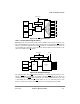
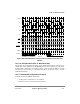
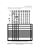
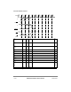
Figure 10-67. DRAM Interface Connection to the 60x Bus (64-Bit Port Size)
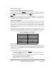
After timings are created, programming the UPM continues with translating these timings
into tables representing the RAM array contents for each possible cycle. When a table is
completed, the global parameters of the UPM must be deÞned for handling the disable
timer (precharge) and the refresh timer relative to Figure 10-67. Table 10-41 shows settings
of different Þelds.
The OR and BR of the speciÞc bank must be initialized according to the address mapping
of the DRAM device used. The MS Þeld should indicate the speciÞc UPM selected to
handle the cycle. The RAM array of the UPM can than be written through use of the
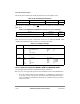
Table 10-41. UPMs Attributes Example
Explanation Field Value
Machine select UPMA BRx[MS] 0b100
Port size 64-bit BRx[PS] 0b00
No write protect (R/W) BRx[WP] 0b0
Refresh timer value (1024 refresh cycles) PURT[PURT] 0x0C
Refresh timer enable MxMR[RFEN] 0b1
Address multiplex size MxMR[AMx] 0b010
Disable timer period MxMR[DSx] 0b01
Select between GPL4 and Wait = GPL4 data sample at clock rising edge MxMR[GPL_x4DIS] 0b0
Burst inhibit device ORx[BI] 0b0
RAS
CAS[0–1]
W
1M x 16
16
A[0–9]
D[0–15]
RAS
CAS[0–1]
W
1M x 16
16
A[0–9]
D[0–15]
MPC8260
BS[0–7]
CS1
BCTL0
A[19–28]
D[0–63]
RAS
CAS[0–1]
W
1M x 16
16
A[0–9]
D[0–15]
RAS
CAS[0–1]
W
1M x 16
16
A[0–9]
D[0–15