
Processor Users Manual


12-28
MPC8260 PowerQUICC II UserÕs Manual
MOTOROLA
Part III. The Hardware Interface
12.4 Instruction Register
The MPC8260Õs JTAG implementation includes the public instructions (EXTEST,
SAMPLE/PRELOAD, and BYPASS) and also supports the CLAMP instruction. One
additional public instruction (HI-Z) can be used to disable all device output drivers. The
MPC8260 includes a 4-bit instruction register (no parity) that consists of a shift register
with four parallel outputs. Data is transferred from the shift register to the parallel outputs
during the update-IR controller state. The four bits are used to decode the Þve unique
instructions listed in Table 12-3.
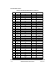
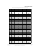
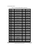
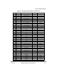
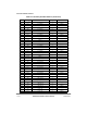
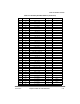
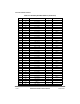
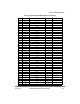
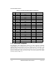
854 o.pin pb[5] io g11.ctl
855 IO.ctl g11.ctl Ñ Ñ
856 i.obs pa[2] io Ñ
857 o.pin pa[2] io g10.ctl
858 IO.ctl g10.ctl Ñ Ñ
859 i.obs pd[6] io Ñ
860 o.pin pd[6] io g9.ctl
861 IO.ctl g9.ctl Ñ Ñ
862 i.obs pc[3] io Ñ
863 o.pin pc[3] io g8.ctl
864 IO.ctl g8.ctl Ñ Ñ
865 i.obs pb[6] io Ñ
866 o.pin pb[6] io g7.ctl
867 IO.ctl g7.ctl Ñ Ñ
868 i.obs pa[3] io Ñ
869 o.pin pa[3] io g6.ctl
870 IO.ctl g6.ctl Ñ Ñ
871 i.obs pd[7] io Ñ
872 o.pin pd[7] io g5.ctl
873 IO.ctl g5.ctl Ñ Ñ
874 i.obs pc[4] io Ñ
875 o.pin pc[4] io g4.ctl
876 IO.ctl g4.ctl Ñ Ñ
877 i.obs pb[7] io Ñ
878 o.pin pb[7] io g3.ctl
Table 12-2. Boundary Scan Bit Definition (Continued)
Bit Cell Type Pin/Cell Name Pin Type Output Control Cell