
Processor Users Manual

13-16 MPC8260 PowerQUICC II UserÕs Manual MOTOROLA
Part IV. Communications Processor Module
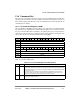
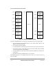
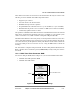
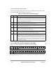
Figure 13-8. Dual-Port RAM Memory Map
The dual-port RAM data bus is 64-bits wide. The RAM is used for six possible tasks:
¥ To store parameters associated with the FCCs, SCCs, MCCs, SMCs, SPI, I
2
C, and
IDMAs in the parameter RAM.
¥ To store buffer descriptors (BDs).
¥ To hold data buffers (optional because data can also be stored in external memory).
¥ For temporary storage of FCC data moving to/from an FCC FIFO (using the BTM)
from/to external memory (using SDMA).
¥ To store RAM microcode for the CP. This feature allows Motorola to add protocols
in the future.
¥ For additional scratch-pad RAM space for user software.
The RAM is designed to serve multiple requests at the same cycle, as long as they are not
in the same bank.
BD/Data/µCode
2 KBytes
Bank #1
0x0000
BD/Data/µCode
2 KBytes
Bank #2
0x0800
BD/Data/µCode
2 KBytes
Bank #3
0x1000
BD/Data/µCode
2 KBytes
Bank #4
0x1800
BD/Data/µCode
2 KBytes
Bank #5
0x2000
BD/Data/µCode
2 KBytes
Bank #6
0x2800
BD/Data
2 KBytes
Bank #7
0x3000
BD/Data
2 KBytes
Bank #8
0x3800
BD/Data/µCode
2 KBytes
Bank #1
0x4000
BD/Data/µCode
2 KBytes
Bank #1
BD/Data/µCode
2 KBytes
Bank #1
BD/Data/µCode
2 KBytes
Bank #1
BD/Data/µCode
2 KBytes
Bank #1
BD/Data/µCode
2 KBytes
Bank #1
BD/Data/µCode
2 KBytes
Bank #1
BD/Data/µCode
2 KBytes
Bank #1
Parameter RAM
2 KBytes
Bank #9
0x8000
Parameter RAM
2 KBytes
Bank #10
0x8800
BD/Data/µCode
2 KBytes
Bank #11
0x9000
BD/Data/µCode
2 KBytes
Bank #1
BD/Data/µCode
2 KBytes
Bank #1
BD/Data/µCode
2 KBytes
Bank #1
FCC Data
2 KBytes
Bank #11
0xB000
FCC Data
2 KBytes
Bank #12
0xB800
Reserved Reserved
(Partially Reserved)