
Processor Users Manual

14-14
MPC8260 PowerQUICC II UserÕs Manual
MOTOROLA
Part IV. Communications Processor Module
First, divide the frame from the start (the sync) to the end of the frame according to the
support that is required:
¥ 8 bits (B1)ÑSCC2
¥ 1 bit (D)ÑSCC1 + strobe 1
¥ 1 bitÑno support
¥ 4 bits (B2)Ñstrobe 2
¥ 4 bits (B2)ÑSMC1
¥ 1 bit (D)ÑSCC1 + strobe 1
Each of these six divisions can be supported by a single SI
x
RAM entry. Thus, six SI
x
RAM
entries are needed. See Table 14-3.
Note that because IDL requires the same routing for both receive and transmit, an exact
duplicate of the above entries should be written to both the receive and transmit sections of
the SI
x
RAM. Then SI
x
MR[CRTx] can be used to instruct the SI
x
RAM to use the same
clock and sync to simultaneously control both sets of SI
x
RAM entries.
14.4.5 Static and Dynamic Routing
The SI
x
RAM has two operating modes for the TDMs:
¥ Static routing. The number of SI
x
RAM entries is determined by the banks the user
relates to the corresponding TDM and is divided into two parts (Rx and Tx). Three
requirements must be met before the new routing takes effect.
Ñ All serial devices connected to the TSA must be disabled.
Ñ SI routing can be modiÞed.
Ñ All appropriate serial devices connected to the TSA must be reenabled.
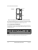
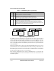
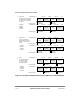
Table 14-3. SI
x
RAM Entry Descriptions
Entry
Number
SI
x
RAM Entry
MCC SWTR SSEL CSEL CNT BYT LST Description
0 0 0 0000 0010 000 1 0 8-bit SCC2
1 0 0 1000 0001 000 0 0 1-bit SCC1 strobe1
2 0 0 0000 0000 000 0 0 1-bit no support
3 0 0 0100 0000 011 0 0 4-bit strobe2
4 0 0 0000 0101 011 0 0 4-bit SMC1
5 0 0 1000 0001 000 0 1 1-bit SCC1 strobe1