
Processor Users Manual

14-30 MPC8260 PowerQUICC II UserÕs Manual MOTOROLA
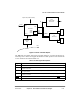
Part IV. Communications Processor Module
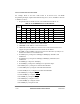
For example, based on the same 10-bit format as in Section 14.4.4, ÒSIx RAM
Programming Example,Ó implement an IDL bus using SCC1, SCC2, and SMC1 connected
to TDMa1 as follows:
1. Program both the Tx and Rx sections of the SIx RAM as in Table 14-10.
2. CMXSI1CR = 0x00. TDMA receive clock is CLK1.
3. CMXSMR = 0x80. SMC1 is connected to the TSA.
4. CMXSCR = 0xC040_0000. SCC1 and SCC2 are connected to the TSA. SCC1
supports the grant mechanism because it handles the D channel.
5. SI1AMR = 0x0145. TDMA grant mode is used with 1-bit frame sync delay in Tx
and Rx and common receive-transmit mode.
6. Set PPARA[6Ð9]. ConÞgures L1TXDa[0], L1RXDa[0], L1TSYNCa, and
L1RSYNCa.
7. Set PSORA[6Ð9]. ConÞgures L1TXDa[0], L1RXDa[0], L1TSYNCa, and
L1RSYNCa.
8. Set PDIRA[9]. ConÞgures L1TXDa[0].
9. Set PODRA[9]. ConÞgures L1TXDa[0] to an open-drain output.
10. Set PPARC[30,31]. ConÞgures L1TCLKa and L1RCLKa.
11. Clear PDIRC[30,31] ConÞgures L1TCLKa and L1RCLKa.
12. Clear PSORC[30,31]. ConÞgures L1TCLKa and L1RCLKa.
13. Set PPARB[17]. ConÞgures L1RQa
.
14. Clear PSORB[17]. ConÞgures L1RQa.
15. Set PDIRB[17]. ConÞgures L1RQa.
16. Set PPARD[13]. ConÞgures L1ST1.
17. Clear PSORD[13]. ConÞgures L1ST1.
18. Set PDIRD[13]. ConÞgures L1ST1.
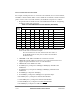
Table 14-10. SIx RAM Entries for an IDL Interface
Entry
Number
SIx RAM Entry
MCC SWTR SSEL CSEL CNT BYT LST Description
0 0 0 0000 0010 000 1 0 8-bit SCC2
1 0 0 0000 0001 000 0 0 1-bit SCC1
2 0 0 0000 0000 000 0 0 1-bit no support
3 0 0 0000 0101 011 1 0 4-bit SMC1
4 0 0 0000 0101 011 1 0 4-bit SMC1
5 0 0 1000 0001 000 0 1 1-bit SCC1 strobe1