
Processor Users Manual

MOTOROLA Chapter 15. CPM Multiplexing 15-15
Part IV. Communications Processor Module
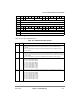
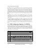
Table 15-6 describes CMXSCR Þelds.
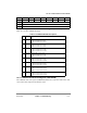
Bits 0 1 2 3 4 5 6 7 8 9 10 11 12 13 14 15
Field GR1 SC1 RS1CS TS1CS GR2 SC2 RS2CS TS2CS
Reset 0000_0000_0000_0000
R/W R/W
Addr 0x11B08
Bits 16 17 18 19 20 21 22 23 24 25 26 27 28 29 30 31
Field GR3 SC3 RS3CS TS3CS GR4 SC4 RS4CS TS4CS
Reset 0000_0000_0000_0000
R/W R/W
Addr 0x11B0A
Figure 15-11. CMX SCC Clock Route Register (CMXSCR)
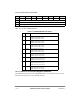
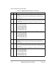
Table 15-6. CMXSCR Field Descriptions
Bits Name Description
0 GR1 Grant support of SCC1
0 SCC1 transmitter does not support the grant mechanism. The grant is always asserted
internally.
1 SCC1 transmitter supports the grant mechanism as determined by the GMx bit of a serial
device channel.
1 SC1 SCC1 connection
0 SCC1 is not connected to the TSA and is either connected directly to the NMSIx pins or is not
used. The choice of general-purpose I/O port pins versus SCCn pins is made in the parallel I/O
control register.
1 SCC1 is connected to TSA of the SIs. The NMSIx pins are available for other purposes.
2Ð4 RS1CS Receive SCC1 clock source (NMSI mode). Ignored if SCC1 is connected to the TSA (SC1 = 1).
000 SCC1 receive clock is BRG1.
001 SCC1 receive clock is BRG2.
010 SCC1 receive clock is BRG3.
011 SCC1 receive clock is BRG4.
100 SCC1 receive clock is CLK11.
101 SCC1 receive clock is CLK12.
110 SCC1 receive clock is CLK3.
111 SCC1 receive clock is CLK4.
5Ð7 TS1CS Transmit SCC1 clock source (NMSI mode). Ignored if SCC1 is connected to the TSA (SC1 = 1).
000 SCC1 transmit clock is BRG1.
001 SCC1 transmit clock is BRG2.
010 SCC1 transmit clock is BRG3.
011 SCC1 transmit clock is BRG4.
100 SCC1 transmit clock is CLK11.
101 SCC1 transmit clock is CLK12.
110 SCC1 transmit clock is CLK3.
111 SCC1 transmit clock is CLK4.