
Processor Users Manual

16-2 MPC8260 PowerQUICC II UserÕs Manual MOTOROLA
Part IV. Communications Processor Module
Each BRG clock source can be BRGCLK, or a choice of two external clocks (selected in
BRGCx[EXTC]). The BRGCLK is an internal signal generated in the MPC8260 clock
synthesizer speciÞcally for the BRGs, the SPI, and the I
2
C internal BRG. Alternatively,
external clock pins can be conÞgured as clock sources. The external source option allows
ßexible baud-rate frequency generation, independent of the system frequency. Additionally,
the external source option allows a single external frequency to be the source for multiple
BRGs. The external source signals are not synchronized internally before being used by the
BRG.
The BRG provides a divide-by-16 option (BRGCx[DIV16]) and a 12-bit prescaler
(BRGCx[CD]) to divide the source clock frequency. The combined source-clock divide
factor can be changed on-the-ßy; however, two changes should not occur within two source
clock periods.
The prescaler output is sent internally to the bank of clocks and can also be output
externally on BRGOn through the parallel I/O ports. If the BRG divides the clock by an
even value, the transitions of BRGOn always occur on the falling edge of the source clock.
If the divide factor is odd, the transitions alternate between the falling and rising edges of
the source clock. Additionally, the output of the BRG can be sent to the autobaud control
block.
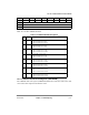
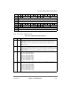
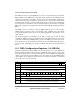
16.1 BRG ConÞguration Registers 1Ð8 (BRGCx)
The BRG conÞguration registers (BRGCx) are shown in Figure 16-2. A reset disables the
BRG and drives the BRGO output clock high. The BRGC can be written at any time with
no need to disable the SCCs or external devices that are connected to BRGO. ConÞguration
changes occur at the end of the next BRG clock cycle (no spikes occur on the BRGO output
clock). BRGC can be changed on-the-ßy; however, two changes should not occur within a
time equal to two source clock periods.
Bit 0 1 2 3 4 5 6 7 8 9 10 11 12 13 14 15
Field Ñ RST EN
Reset 0000_0000_0000_0000
R/W R/W
Addr 0x119F0 (BRGC1), 0x119F4 (BRGC2), 0x119F8 (BRGC3), 0x119FC (BRGC4),
0x115F0 (BRGC5), 0x115F4 (BRGC6), 0x115F8 (BRGC7), 0x115FC (BRGC8)
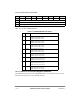
Bit 16 17 18 19 20 21 22 23 24 25 26 27 28 29 30 31
Field EXTC ATB CD DIV16
Reset 0000_0000_0000_0000
R/W R/W
Addr 0x119F22 (BRGC1), 0x119F6 (BRGC2), 0x119FA (BRGC3), 0x119FE (BRGC4),
0x115F2 (BRGC5), 0x115F6 (BRGC6), 0x115FA (BRGC7), 0x115FE (BRGC8)
Figure 16-2. Baud-Rate Generator Configuration Registers (BRGCx)