
Processor Users Manual

17-4 MPC8260 PowerQUICC II UserÕs Manual MOTOROLA
Part IV. Communications Processor Module
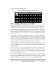
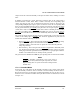
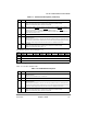
Figure 17-2. Timer Cascaded Mode Block Diagram
If TGCR[CAS] = 1, the two timers function as a 32-bit timer with a 32-bit TRR, TCR, and
TCN. In this case, TMR1 and/or TMR3 are ignored, and the modes are deÞned using TMR2
and/or TMR4. The capture is controlled from TIN2 or TIN4 and the interrupts are generated
from TER2 or TER4. In cascaded mode, the combined TRR, TCR, and TCN must be
referenced with 32-bit bus cycles.
17.2.2 Timer Global ConÞguration Registers (TGCR1 and TGCR2)
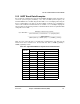
The timer global conÞguration registers (TGCR1 and TGCR2), shown in Figure 17-3 and
Figure 17-4, contain conÞguration parameters used by the timers. These registers allow
simultaneous starting and stopping of a pair of timers (1 and 2 or 3 and 4) if one bus cycle
is used.
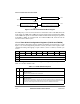
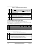
Table 17-1 describes TGCR1 Þelds.
Bits 0 1 2 3 4 5 6 7
Field CAS2 Ñ STP2 RST2 GM1 Ñ STP1 RST1
Reset 0000_0000
R/W R/W
Addr 0x10D80
Figure 17-3. Timer Global Configuration Register 1 (TGCR1)
Table 17-1. TGCR1 Field Descriptions
Bits Name Description
0 CAS2 Cascade timers.
0 Normal operation.
1 Timers 1 and 2 cascade to form a 32-bit timer.
1 Ñ Reserved, should be cleared.
2 STP 2 Stop timer.
0 Normal operation.
1 Reduce power consumption of the timer. This bit stops all clocks to the timer, except the clock
from the internal bus interface, which allows the user to read and write timer registers. The clocks
to the timer remain stopped until the user clears this bit or a hardware reset occurs.
Timer1
Timer2
Timer3
Timer4
Capture
Capture
Clock
Clock
TRR, TCR, TCN connected to D[16Ð31] TRR, TCR, TCN connected to D[0Ð15]
TRR, TCR, TCN connected to D[0Ð15] TRR, TCR, TCN connected to D[16Ð31]