
Processor Users Manual

MOTOROLA Chapter 17. Timers 17-7
Part IV. Communications Processor Module
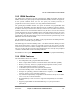
17.2.4 Timer Reference Registers (TRR1ÐTRR4)
Each timer reference register (TRR1ÐTRR4), shown in Figure 17-6, contains the timeoutÕs
reference value. The reference value is not reached until TCNx increments to equal the
timeout reference value.
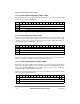
10 OM Output mode
0 Active-low pulse on T
OUTx for one timer input clock cycle as deÞned by the ICLK bits. Thus,
T
OUTx may be low for one general system clock period, one general system clock/16 period, or
one TINx clock cycle period. T
OUTx changes occur on the rising edge of the system clock.
1 Toggle T
OUTx. TOUTx changes occur on the rising edge of the system clock.
11 ORI Output reference interrupt enable.
0 Disable interrupt for reference reached (does not affect interrupt on capture function).
1 Enable interrupt upon reaching the reference value.
12 FRR Free run/restart.
0 Free run. The timer count continues to increment after the reference value is reached.
1 Restart. The timer count is reset immediately after the reference value is reached.
13Ð14 ICLK Input clock source for the timer.
00 Internally cascaded input. For TMR1, the timer 1 input is the output of timer 2. For TMR3, the
timer 3 input is the output of timer 4. For TMR2 and TMR4, this selection means no input clock is
provided to the timer.
01 Internal general system clock.
10 Internal general system clock divided by 16.
11 Corresponding TINx: TIN1, TIN2, TIN3, or TIN4 (falling edge).
15 GE Gate enable.
0 TGA
TEx is ignored.
1 TGA
TEx is used to control the timer.
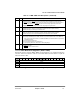
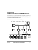
Bit 0 1 2 3 4 5 6 7 8 9 10 11 12 13 14 15
Field Timeout reference value
Reset 0xFFFF
R/W R/W
Addr 0x10D94 (TRR1), 0x10D96 (TRR2), 0x10DA4 (TRR3), 0x10DA6 (TRR4)
Figure 17-6. Timer Reference Registers (TRR1ÐTRR4)
Table 17-3. TMRIÐTMR4 Field Descriptions (Continued)
Bits Name Description