
Processor Users Manual

18-28 MPC8260 PowerQUICC II UserÕs Manual MOTOROLA
Part IV. Communications Processor Module
18.11 Programming the Parallel I/O Registers
The parallel I/O registers control the use of the external pins of the chip. Each pin can be
used for different purposes. See Table 18-12, Table 18-13 and Table 18-14 (optional) for
the proper parallel I/O register programming dedicating the proper external ports to the four
IDMA channelsÕ external I/O signals.
Each port is controlled by Þve I/O registers: PPAR, PSOR, PDIR, PODR, and PDAT. Each
bit in these registers controls the external pin of the same location.
¥ PPARC selects the pins general purpose(0)/dedicated(1) mode for port C.
¥ PDIRC select the pins input or inout (0)/output(1) mode for port C.
¥ PODRC selects the open drain pins for port C.
¥ PSORC selects the pins dedicated1(0)/dedicated2(1) mode for port C.
¥ PPARA, PDIRA, PODRA, and PSORA control port A in the same way.
¥ PPARD, PDIRD, PODRD, and PSORD control port D in the same way.
¥ The default is the value that is seen by the IDMA channel on the pin (input or inout
mode onlyÑPDIR[PN] = 0) if a PSORx register bit is set to the complement value
of the value in Table 18-12, Table 18-13 and Table 18-14. See Section 35.2, ÒPort
Registers.Ó
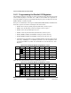
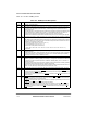
Table 18-13 describes parallel I/O register programming for port A.
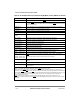
Table 18-12. Parallel I/O Register ProgrammingÑPort C
Channel Signal Pin PPARC PDIRC PODRC PSORC Default
IDMA1 DREQ1
(I) PC[0] 1000 GND
DACK1 (O) PC[23] 1101 Ñ
DONE1 (I/O) PC[22] 1011 VDD
IDMA2 DREQ2 (I) PC[1] 1000 GND
DACK2 (O) PC[3] 1101 Ñ
DONE2 (I/O) PC[2] 1011 VDD
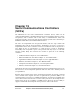
Table 18-13. Parallel I/O Register ProgrammingÑPort A
Channel Signal Pin PPARA PDIRA PODRA PSORA Default
IDMA3 DREQ3
(I) PA[0] 1001 GND
DACK3 (O) PA[2] 1101 Ñ
DONE3 (I/O) PA[1] 1011 VDD
IDMA4 DREQ4 (I) PA[5] 1001 GND
DACK4 (O) PA[3] 1101 Ñ
DONE4 (I/O) PA[4] 1011 VDD