
Processor Users Manual


MOTOROLA Chapter 19. Serial Communications Controllers (SCCs) 19-13
Part IV. Communications Processor Module
set by the core (the buffer is empty). After using a descriptor, the CPM clears E (not empty)
and does not reuse a BD until it has been processed by the core. However, in continuous
mode (CM), E remains set. When the CPM discovers a descriptorÕs W bit set (indicating it
is the last BD in the circular BD table), it returns to the beginning of the table when it is
time to move to the next buffer.
19.3 SCC Parameter RAM
Each SCC parameter RAM area begins at the same offset from each SCC base area.
Section 19.3.1, ÒSCC Base Addresses,Ó describes the SCCÕs base addresses. The protocol-
speciÞc portions of the SCC parameter RAM are discussed in the speciÞc protocol
descriptions and the part that is common to all SCC protocols is shown in Table 19-4.
Some parameter RAM values must be initialized before the SCC can be enabled. Other
values are initialized or written by the CPM. Once initialized, most parameter RAM values
do not need to be accessed because most activity centers around the descriptors rather than
the parameter RAM. However, if the parameter RAM is accessed, note the following:
¥ Parameter RAM can be read at any time.
¥ Tx parameter RAM can be written only when the transmitter is disabledÑafter a
STOP TRANSMIT command and before a RESTART TRANSMIT command or after the
buffer/frame Þnishes transmitting after a
GRACEFUL STOP TRANSMIT command and
before a
RESTART TRANSMIT command.
¥ Rx parameter RAM can be written only when the receiver is disabled. Note the
CLOSE RXBD command does not stop reception, but it does allow the user to extract
data from a partially full Rx buffer.
¥ See Section 19.3.8, ÒReconÞguring the SCCs.Ó
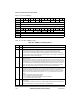
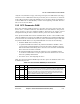
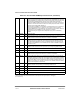
Table 19-4 shows the parameter RAM map for all SCC protocols. Boldfaced entries must
be initialized by the user.
Table 19-4. SCC Parameter RAM Map for All Protocols
Offset
1
Name Width Description
0x00 RBASE Hword Rx/TxBD table base addressÑoffset from the beginning of dual-port RAM. The BD
tables can be placed in any unused portion of the dual-port RAM. The CPM starts BD
processing at the top of the table. (The user deÞnes the end of the BD table by setting
the W bit in the last BD to be processed.) Initialize these entries before enabling the
corresponding channel. Erratic operations occur if BD tables of active SCCs overlap.
Values in RBASE and TBASE should be multiples of eight.
0x02 TBASE Hword
0x04 RFCR Byte Rx function code. See Section 19.3.2, ÒFunction Code Registers (RFCR and TFCR).Ó
0x05 TFCR Byte Tx function code. See Section 19.3.2, ÒFunction Code Registers (RFCR and TFCR).Ó