
Processor Users Manual

MOTOROLA Chapter 19. Serial Communications Controllers (SCCs) 19-15
Part IV. Communications Processor Module
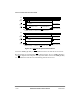
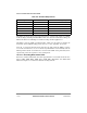
19.3.1 SCC Base Addresses
The CPM maintains a section of RAM called the parameter RAM, which contains many
parameters for the operation of the FCCs, SCCs, SMCs, SPI, I
2
C, and IDMA channels.
SCC base addresses are described in Table 19-5.
The exact deÞnition of the parameter RAM is contained in each protocol subsection
describing a device that uses a parameter RAM. For example, the Ethernet parameter RAM
is deÞned differently in some locations from the HDLC-speciÞc parameter RAM.
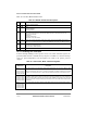
19.3.2 Function Code Registers (RFCR and TFCR)
There are eight separate function code registers for the four SCC channels, four for Rx
buffers (RFCR1ÐRFCR4) and four for Tx buffers (TFCR1ÐTFCR4). The function code
registers contain the transaction speciÞcation associated with SDMA channel accesses to
external memory. Figure 19-8 shows the register format.
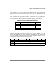
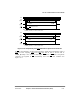
Table 19-5. Parameter RAMÑSCC Base Addresses
Page Address
1
1
Offset from RAM_Base
Peripheral Size (Bytes)
1 0x8000 SCC1 256
2 0x8100 SCC2 256
3 0x8200 SCC3 256
4 0x8300 SCC4 256
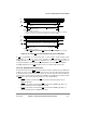
Bit 0 1 2 3 4 5 6 7
Field Ñ GBL BO TC2 DTB Ñ
Reset 0000_0000_0000_0000
R/W R/W
Addr SCCx base + 0x04 (RFCRx); SCCx base + 0x05 (TFCRx)
Figure 19-8. Function Code Registers (RFCR and TFCR)