
Processor Users Manual


MOTOROLA Chapter 28. Fast Communications Controllers (FCCs) 28-3
Part IV. Communications Processor Module
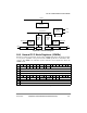
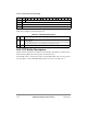
Figure 28-1. FCC Block Diagram
28.2 General FCC Mode Registers (GFMRx)
Each FCC contains a general FCC mode register (GFMRx) that deÞnes all options common
to every FCC, regardless of the protocol. Some GFMR operations are described in later
sections. The GFMRx are read/write registers cleared at reset. Figure 28-2 shows the
GFMR format.
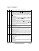
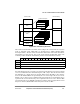
Bits 0 1 2 3 4 5 6 7 8 9 10 11 12 13 14 15
Field DIAG TCI TRX TTX CDP CTSP CDS CTSS Ñ
Reset 0000_0000_0000_0000
R/W R/W
Addr 0x11300 (GFMR1), 0x11320 (GFMR2), 0x11340 (GFMR3)
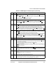
Bits 16 17 18 19 20 21 22 23 24 25 26 27 28 29 30 31
Field SYNL RTSM RENC REVD TENC TCRC ENR ENT MODE
Reset 0000_0000_0000_0000
R/W R/W
Addr 0x11302 (GFMR1), 0x11322 (GFMR2), 0x11342 (GFMR3)
Figure 28-2. General FCC Mode Register (GFMR)
Control
Registers
ShifterShifter Delimiter
Clock
Generator
Delimiter
Decoder
Encoder
Receive
Control
Unit
Transmit
Control
Unit
Receive
Data
FIFO
Transmit
Data
FIFO
Modem Lines
Modem Lines
60x Bus
Peripheral Bus
TCLK
RCLK
Internal Clocks
RXD
TXD