
Processor Users Manual

29-39 MPC8260 PowerQUICC II UserÕs Manual MOTOROLA
Part IV. Communications Processor Module
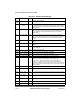
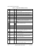
0x6C BD_BASE_EXT Word BD table base address extension. BD_BASE_EXT[0Ð7] holds the 8 most-
signiÞcant bits of the Rx/Tx BD table base address. BD_BASE_EXT[8Ð31]
should be zero. User-deÞned.
0x70 VPT_BASE /
EXT_CAM_BASE
Word Base address of the address compression VP table/external CAM. User-
deÞned.
0x74 VCT_BASE Word Base address of the address compression VC table. User-deÞned.
0x78 VPT1_BASE /
EXT_CAM1_BASE
Word Base address of the address compression VP1 table/EXT CAM1. User-
deÞned.
0x7C VCT1_BASE Word Base address of the address compression VC1 table. User-deÞned.
0x80 VP_MASK Hword VP mask for address compression lookup. User-deÞned.
0x82 VCIF Hword VCI Þltering enable bits. When cells with VCI = 3, 4, 6, 7-15 are received and
the associated VCIF bit = 1 the cell is sent to the raw cell queue. VCIF[0Ð2, 5]
should be zero. See Section 29.10.1.2, ÒVCI Filtering (VCIF).Ó
0x84 GMODE Hword Global mode. User-deÞned. See Section 29.10.1.3, ÒGlobal Mode Entry
(GMODE).Ó
0x86 COMM_INFO Hword The information Þeld associated with the last host command. User-deÞned.
See Section 29.14, ÒATM Transmit Command.Ó
0x88 Hword
0x8A Hword
0x8C Ñ Word Reserved, should be cleared.
0x90 CRC32_PRES Word Preset for CRC32. Initialize to 0xFFFF_FFFF.
0x94 CRC32_MASK Word Constant mask for CRC32. Initialize to 0xDEBB_20E3.
0x98 AAL1_SNPT_BASE Hword AAL1 SNP protection look-up table base address. (AAL1 only.) The 32-byte
table resides in dual-port RAM. AAL1_SNPT_BASE must be halfword-aligned.
User-deÞned offset from dual-port RAM base. See Section 29.10.6, ÒAAL1
Sequence Number (SN) Protection Table (AAL1 Only).Ó
0x9A Ñ Hword Reserved, should be cleared.
0x9C SRTS_BASE Word External SRTS logic base address. AAL1 only. Should be 16-byte aligned. The
four least-signiÞcant bits are taken from SRTS_DEVICE in the AAL1-speciÞc
area of the connection table entries.
0xA0 IDLE/
UNASSIGN_BASE
Hword Idle/unassign cell base address. Points to dual-port RAM area contains idle/
unassign cell template (little-endian format). Should be 64-byte aligned. User-
deÞned offset from dual-port RAM base. The ATM header should be
0x0000_0000 or 0x0100_0000 (CLP=1).
0xA0 IDLE/
UNASSIGN_SIZE
Hword Idle/unassign cell size. 52 in regular mode; 53Ð64 in UDC mode.
0xA4 EPAYLOAD Word Reserved payload. Initialize to 0x6A6A_6A6A.
0xA8 Trm Word (ABR only) The upper bound on the time between F-RM cells for an active
source. TM 4.0 deÞnes the Trm period as 100 msec. The Trm value is deÞned
by the system clock and the time stamp timer prescaler; see Section 13.3.7,
ÒRISC Time-Stamp Control Register (RTSCR).Ó For time stamp prescalar of
1µs, program Trm to be 100 ms/1µs = 100,000.
Table 29-11. ATM Parameter RAM Map (Continued)
Offset
1
Name Width Description