
Processor Users Manual

29-40 MPC8260 PowerQUICC II UserÕs Manual MOTOROLA
Part IV. Communications Processor Module
29.10.1.1 Determining UEAD_OFFSET (UEAD Mode Only)
The UEAD_OFFSET value is based on the position of the user-deÞned extended address
(UEAD) in the UDC extra header. Table 29-12 shows how to determine UEAD_OFFSET:
Þrst determine the halfword-aligned location of the UEAD, and then read the
corresponding UEAD_OFFSET value.
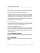
29.10.1.2 VCI Filtering (VCIF)
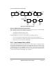
VCI Þltering enable bits are shown in Figure 29-22.
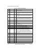
Table 29-13 describes the operation of the VCI Þltering enable bits.
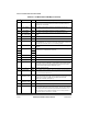
0xAC Nrm Hword (ABR only) Controls the maximum cells the source may send for each F-RM
cell. Set to 32 cells.
0xAE Mrm Hword (ABR only) Controls the bandwidth between F-RM, B-RM and user data cell.
Set to 2 cells.
0xB0 TCR Hword (ABR only) Tag cell rate. The minimum cell rate allowed for all ABR channels.
An ABR channel whose ACR is less than TCR sends only out-of-rate F-RM
cells at TCR. Should be set to 10 cells/sec as deÞned in the TM 4.0. Uses the
ATMF TM 4.0 ßoating-point format. Note that the APC minimum cell rate
(MCR) should be at least TCR.
0xB2 ABR_RX_TCTE Hword (ABR only) Points to total of 16 bytes reserved dual-port RAM area used by the
CP. Should be double-word aligned. User-deÞned offset from dual-port RAM
base.
1
Offset from FCC base: 0x8400 (FCC1) and 0x8500 (FCC2); see Section 13.5.2, ÒParameter RAM.Ó
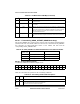
Table 29-12. UEAD_OFFSETs for Extended Addresses in the UDC Extra Header
Bits/
Header Offset
0Ð15 16Ð31
0x0 UEAD_OFFSET = 0x2 UEAD_OFFSET = 0x0
0x4 UEAD_OFFSET = 0x6 UEAD_OFFSET = 0x4
0x8 UEAD_OFFSET = 0xA UEAD_OFFSET = 0x8
Bits 0 1 2 3 4 5 6 7 8 9 10 11 12 13 14 15
Field 0 0 0 VC3 VC4 0 VC6 VC7 VC8 VC9 VC10 VC11 VC12 VC13 VC14 VC15
Figure 29-22. VCI Filtering Enable Bits
Table 29-13. VCI Filtering Enable Field Descriptions
Bits Name Description
0Ð2, 5 Ñ Clear these bits.
3, 4, 6,
7Ð15
VCx VCI Þltering enable
0 Do not send cells with this VCI to the raw cell queue.
1 Send cells with this VCI to the raw cell queue.
Table 29-11. ATM Parameter RAM Map (Continued)
Offset
1
Name Width Description