
Processor Users Manual


31-14 MPC8260 PowerQUICC II UserÕs Manual MOTOROLA
Part IV. Communications Processor Module
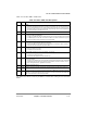
The remaining TxBD parameters are as follows:
¥ Data length is the number of bytes the HDLC controller should transmit from this
data buffer; it is never modiÞed by the CP. The value of this Þeld should be greater
than zero.
¥ Tx data buffer pointer. The transmit buffer pointer, which contains the address of the
associated data buffer, can be even or odd. The buffer can reside in internal or
external memory. This value is never modiÞed by the CP.
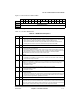
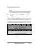
31.9 HDLC Event Register (FCCE)/Mask Register
(FCCM)
The FCCE is used as the HDLC event register when the FCC operates as an HDLC
controller. The FCCE reports events recognized by the HDLC channel and generates
interrupts. On recognition of an event, the HDLC controller sets the corresponding FCCE
bit. FCCE bits are cleared by writing ones; writing zeros does not affect bit values. All
unmasked bits must be cleared before the CP clears the internal interrupt request.
Interrupts generated by the FCCE can be masked in the HDLC mask register (FCCM),
which has the same bit format as FCCE. If an FCCM bit = 1, the corresponding interrupt
in the event register is enabled. If the bit is 0, the interrupt is masked.
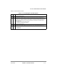
Table 31-9 describes FCCE/FCCM Þelds.
Bits 0 1 2 3 4 5 6 7 8 9 10 11 12 13 14 15
Field Ñ GRA Ñ TXE RXF BSY TXB RXB
Reset 0000_0000_0000_0000
R/W R/W
Addr 0x11310 (FCCE1), 0x11330 (FCCE2), 0x11350 (FCCE3)/
0x11314 (FCCM1), 0x11334 (FCCM2), 0x11354 (FCCM3)
Bits 16 17 18 19 20 21 22 23 24 25 26 27 28 29 30 31
Field Ñ FLG IDL Ñ
Reset 0000_0000_0000_0000
R/W R/W
Addr 0x11312 (FCCE1), 0x11332 (FCCE2), 0x11352 (FCCE3)/
0x11316 (FCCM1), 0x11336 (FCCM2), 0x11356 (FCCM3)
Figure 31-7. HDLC Event Register (FCCE)/Mask Register (FCCM)