
Processor Users Manual

34-6 MPC8260 PowerQUICC II UserÕs Manual MOTOROLA
Part IV. Communications Processor Module
An MPC8260 I
2
C controller attempting a master read request could simultaneously be
targeted for an external master write (slave read). Both operations trigger the controllerÕs
I2CER[RXB] event, but only one operation wins the bus arbitration. To determine which
operation caused the interrupt, software must verify that its transmit operation actually
completed before assuming that the received data is the result of its read operation.
Problems could also arise if the MPC8260's I
2
C controller master sets up a transmit buffer
and BD for a write request, but then is the target of a read request from another master.
Without software precautions, the I
2
C controller responds to the other master with the
transmit buffer originally intended for its own write request. To avoid this situation, a
higher-level handshake protocol must be used. For example, a master, before reading a
slave, writes the slave with a description of the requested data (which register should be
read, for example). This operation is typical with many I
2
C devices.
34.4 I
2
C Registers
The following sections describe the I
2
C registers.
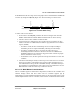
34.4.1 I
2
C Mode Register (I2MOD)
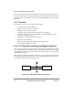
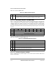
The I
2
C mode register, shown in Figure 34-6, controls the I
2
C modes and clock source.
Table 34-1 describes I2MOD bit functions.
Bit 0 1 2 3 4 5 6 7
Field Ñ REVD GCD FLT PDIV EN
Reset 0000_0000
R/W R/W
Addr 0x11860
Figure 34-6. I
2
C Mode Register (I2MOD)
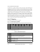
Table 34-1. I2MOD Field Descriptions
Bits Name Description
0Ð1 Ñ Reserved and should be cleared.
2 REVD Reverse data. Determines the Rx and Tx character bit order.
0 Normal operation. The msb (bit 0) of a character is transferred Þrst.
1 Reverse data. the lsb (bit 7) of a character is transferred Þrst.
Note: Clearing REVD is strongly recommended to ensure consistent bit ordering across devices.
3 GCD General call disable. Determines whether the receiver acknowledges a general call address.
0 General call address is enabled.
1 General call address is disabled.
4 FLT Clock Þlter. Determines if the I
2
C input clock SCL is Þltered to prevent spikes in a noisy environment.
0 SCL is not Þltered.
1 SCL is Þltered by a digital Þlter.