
Processor Users Manual

MOTOROLA Chapter 34. I2C Controller 34-7
Part IV. Communications Processor Module
34.4.2 I
2
C Address Register (I2ADD)
The I
2
C address register, shown in Figure 34-7, holds the address for this I
2
C port.
Table 34-2 describes I2CADD Þelds.
34.4.3 I
2
C Baud Rate Generator Register (I2BRG)
The I
2
C baud rate generator register, shown in Figure 34-8, sets the divide ratio of the I
2
C
BRG.
5Ð6 PDIV Predivider. Selects the clock division factor before it is input into the I
2
C BRG. The clock source for the
I
2
C BRG is the BRGCLK generated from the CPM clock; see Section 9.8, ÒSystem Clock Control
Register (SCCR).Ó
00 BRGCLK/32
01 BRGCLK/16
10 BRGCLK/8
11 BRGCLK/4
Note: To both save power and reduce noise susceptibility, select the PDIV with the largest division
factor (slowest clock) that still meets performance requirements.
7 EN Enable I
2
C operation.
0I
2
C is disabled. The I
2
C is in a reset state and consumes minimal power.
1I
2
C is enabled. Do not change other I2MOD bits when EN is set.
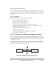
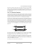
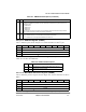
Bit 0 1 2 3 4 5 6 7
Field SAD Ñ
Reset 0000_0000
R/W R/W
Addr 0x11864
Figure 34-7. I
2
C Address Register (I2ADD)
Table 34-2. I2ADD Field Descriptions
Bits Name Description
0Ð6 SAD Slave address 0Ð6. Holds the slave address for the I
2
C port.
7 Ñ Reserved and should be cleared.
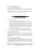
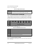
Bit 0 1 2 3 4 5 6 7
Field DIV
Reset 1111_1111
R/W R/W
Addr 0x11868
Figure 34-8. I
2
C Baud Rate Generator Register (I2BRG)
Table 34-1. I2MOD Field Descriptions (Continued)
Bits Name Description