
Processor Users Manual

MOTOROLA Chapter 35. Parallel I/O Ports 35-3
Part IV. Communications Processor Module
to PDATx is still stored in the output latch, but is prevented from reaching the port pin. In
this case, when PDATx is read, the state of the port pin is read.
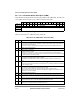
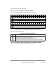
35.2.3 Port Data Direction Registers (PDIRAÐPDIRD)
The port data direction register(PDIR), shown in Figure 35-3, is cleared at system reset.
Table 35-2 describes PDIR Þelds.
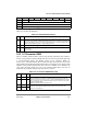
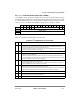
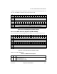
Bits 0 1 2 3 4 5 6 7 8 9 10 11 12 13 14 15
Field D0
1
D1
1
D2
1
D3
1
D4 D5 D6 D7 D8 D9 D10 D11 D12 D13 D14 D15
Reset Ñ
R/W R/W
Addr 0x10D10 (PDATA), 0x10D30 (PDATB), 0x10D50 (PDATC), 0x10D70 (PDATD)
Bits 16 17 18 19 20 21 22 23 24 25 26 27 28 29 30 31
Field D16 D17 D18 D19 D20 D21 D22 D23 D24 D25 D26 D27 D28 D29 D30 D31
Reset Ñ
R/W R/W
Addr 0x10D12 (PDATA), 0x10D32 (PDATB), 0x10D52 (PDATC), 0x10D72 (PDATD)
1
These bits are valid for PDATA and PDATC only
Figure 35-2. Port Data Registers (PDATAÐPDATD)
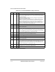
Bits 0 1 2 3 4 5 6 7 8 9 10 11 12 13 14 15
Field DR0
1
DR1
1
DR2
1
DR3
1
DR4 DR5 DR6 DR7 DR8 DR9 DR10 DR11 DR12 DR13 DR14 DR15
Reset 0000_0000_0000_0000
R/W R/W
Addr 0x10D00 (PDIRA), 0x10D20 (PDIRB), 0x10D40 (PDIRC), 0x10D60 (PDIRD)
Bits 16 17 18 19 20 21 22 23 24 25 26 27 28 29 30 31
Field DR16 DR17 DR18 DR19 DR20 DR21 DR22 DR23 DR24 DR25 DR26 DR27 DR28 DR29 DR30 DR31
Reset 0000_0000_0000_0000
R/W R/W
Addr 0x10D02 (PDIRA), 0x10D22 (PDIRB), 0x10D42 (PDIRC), 0x10D62 (PDIRD)
1
These bits are valid for PDIRA and PDIRC only
Figure 35-3. Port Data Direction Register (PDIR)
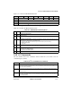
Table 35-2. PDIR Field Descriptions
Bits Name Description
0Ð31 DRx Direction. Indicates whether a pin is used as an input or an output. Note that bits DR0ÐDR3 are valid
for PDIRA and PDIRC only.
0 The corresponding pin is an input.
1 The corresponding pin is an output.