
Processor Users Manual

35-4 MPC8260 PowerQUICC II UserÕs Manual MOTOROLA
Part IV. Communications Processor Module
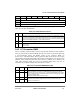
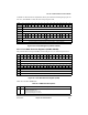
35.2.4 Port Pin Assignment Register (PPAR)
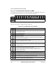
The port pin assignment register (PPAR) is cleared at system reset.
Table 35-2 describes PPARx Þelds.
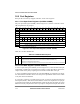
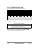
35.2.5 Port Special Options Registers AÐD (PSORAÐPSORD)
Figure 35-5 shows the port special options registers (PSORx).
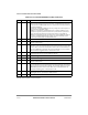
Bits 0 1 2 3 4 5 6 7 8 9 10 11 12 13 14 15
Field DD0
1
DD1
1
DD2
1
DD3
1
DD4 DD5 DD6 DD7 DD8 DD9 DD10 DD11 DD12 DD13 DD14 DD15
Reset 0000_0000_0000_0000
R/W R/W
Addr 0x10D04 (PPARA), 0x10D24 (PPARB), 0x10D44 (PPARC), 0x10D64 (PPARD)
Bits 16 17 18 19 20 21 22 23 24 25 26 27 28 29 30 31
Field DD16 DD17 DD18 DD19 DD20 DD21 DD22 DD23 DD24 DD25 DD26 DD27 DD28 DD29 DD30 DD31
Reset 0000_0000_0000_0000
R/W R/W
Addr 0x10D06 (PPARA), 0x10D26 (PPARB), 0x10D46 (PPARC), 0x10D66 (PPARD)
1
These bits are valid for PPARA and PPARC only
Figure 35-4. Port Pin Assignment Register (PPARAÐPPARD)
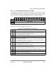
Table 35-3. PPAR Field Descriptions
Bits Name Description
0Ð31 DDx Dedicated enable. Indicates whether a pin is a general-purpose I/O or a dedicated peripheral pin.
Note that bits DD0ÐDD3 are valid for PPARA and PPARC only.
0 General-purpose I/O. The peripheral functions of the pin are not used.
1 Dedicated peripheral function. The pin is used by the internal module. The on-chip peripheral
function to which it is dedicated can be determined by other bits such as those is the PDIR.