
Processor Users Manual

35-6 MPC8260 PowerQUICC II UserÕs Manual MOTOROLA
Part IV. Communications Processor Module
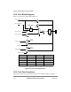
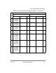
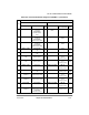
35.3 Port Block Diagram
Figure 35-6 shows the functional block diagram.
Figure 35-6. Port Functional Operation
35.4 Port Pins Functions
Each pin can operate as a general purpose I/O pin or as a dedicated input or output pin.
Pin
PDATx
Default
Input IN1
Default
Input IN2
To DED IN1
To DED IN2
From DED OUT2
PDATx Read
0
1
0
1
PPAR & PSOR & PDIR
PPAR & PSOR & PDIR
Open
Drain
Control
EN
PODR
0
Latch
From DED OUT1
PSOR
1
0
1
PDATx Write
To/from internal bus
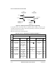
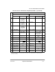
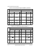
Register Name 0 1 Description
PPARx General purpose Dedicated Port pin assignment
PSORx Dedicated 1 Dedicated 2 Special operation
PDIRx Input Output Direction
1
1
Bidirectional signals must be programmed as inputs (PDIR = 0).
PODRx Regular Open drain
PDATx 0 1 Data
Read
To/from peripheral bus
PDIR
PPAR