
Processor Users Manual

MOTOROLA Chapter 35. Parallel I/O Ports 35-11
Part IV. Communications Processor Module
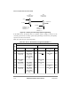
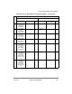
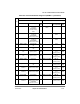
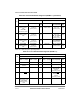
PA12 FCC1: RxD[2]
UTOPIA 8
FCC1: RxD[10]
UTOPIA 16
GND MSNUM[3]
1
PA11 FCC1: RxD[1]
UTOPIA 8
FCC1: RxD[9] FCC1
UTOPIA 16
GND MSNUM[4]
1
PA10 FCC1: RxD[0]
UTOPIA 8
FCC1: RxD[8]
UTOPIA 16
GND MSNUM[5]
1
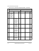
PA 9 SMC2: SMTXD TDM_A1: L1TXD[0]
Output
GND
PA 8
SMC2: SMRXD
(primary option)
by PD4 TDM_A1: L1RXD[0]
Input, nibble
TDM_A1: L1RXD
Inout, serial
GND
PA 7
SMC2: SMSYN
(primary option)
by PC0 TDM_A1: L1TSYNC/
GRANT
GND
PA 6
TDM_A1: L1RSYNC GND
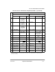
PA 5
SCC2: RSTRT FCC2: RxAddr[2]
MPHY master
IDMA4: DREQ GND
PA 4
FCC2: RxAddr[1]
MPHY master
SCC2: REJECT VDD IDMA4: DONE
Inout
VDD
PA 3
FCC2: RxAddr[0]
MPHY master
CLK19 GND IDMA4: DACK TDM_A2: L1RXD[1]
Nibble
GND
PA 2
FCC2: TxAddr[0]
MPHY master
CLK20 GND IDMA3: DACK
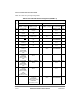
PA 1 FCC2: TxAddr[1]
MPHY master
SCC1: REJECT VDD IDMA3: DONE
Inout
VDD
PA 0
SCC1: RSTRT FCC2: TxAddr[2]
MPHY master
IDMA3: DREQ GND
1
MSNUM[0Ð4] is the sub-block code of the peripheral controller using SDMA; MSNUM[5] indicates which section,
transmit or receive, is active during the transfer. See Section 18.2.4, ÒSDMA Transfer Error MSNUM Registers
(PDTEM and LDTEM).Ó
Table 35-5. Port AÑDedicated Pin Assignment (PPARA = 1) (Continued)
Pin
Pin Function
PSORA = 0 PSORA = 1
PDIRA = 1 (Output) PDIRA = 0 (Input)
Default
Input
PDIRA = 1 (Output)
PDIRA = 0 (Input, or
Inout if SpeciÞed)
Default
Input