MVME197LE Single Board Computer Installation Guide (MVME197LEIG/D1)
Notice While reasonable efforts have been made to assure the accuracy of this document, Motorola, Inc. assumes no liability resulting from any omissions in this document, or from the use of the information obtained therein. Motorola reserves the right to revise this document and to make changes from time to time in the content hereof without obligation of Motorola to notify any person of such revision or changes.
Preface This document provides a general board level hardware description, hardware preparation and installation instructions, debugger general information, and instructions on using the debugger for the MVME197LE Single Board Computer. This document is intended for anyone who wants to design OEM systems, supply additional capability to an existing compatible system, or work in a lab environment for experimental purposes. A basic knowledge of computers and digital logic is assumed.
Data and address sizes are defined as follows: ❏ A byte is eight bits, numbered 0 through 7, with bit 0 being the least significant. ❏ A two-byte is 16 bits, numbered 0 through 15, with bit 0 being the least significant. For the MVME197series and other RISC modules, this is called a half-word. ❏ A four-byte is 32 bits, numbered 0 through 31, with bit 0 being the least significant. For the MVME197 series and other RISC modules, this is called a word.
Related Documentation The following publications are applicable to the MVME197 module series and may provide additional helpful information. If not shipped with this product, they may be purchased by contacting your Motorola sales office.
2. Although not shown in the above list, each Motorola Computer Group manual publication number is suffixed with characters which represent the revision level of the document, such as “/D2” (the second revision of a manual); a supplement bears the same number as the manual but has a suffix such as “/A1” (the first supplement to the manual).
The computer programs stored in the Read Only Memory of this device contain material copyrighted by Motorola Inc., first published 1991, and may be used only under license such as the License for Computer Programs (Article 14) contained in Motorola’s Terms and Conditions of Sale, Rev. 1/79. Motorola® and the Motorola symbol are registered trademarks of Motorola, Inc. Delta Series, M88000, SYSTEM V/88, VMEmodule, VMEsystem, and197bug are trademarks of Motorola, Inc.
SAFETY SUMMARY SAFETY DEPENDS ON YOU The following general safety precautions must be observed during all phases of operation, service, and repair of this equipment. Failure to comply with these precautions or with specific warnings elsewhere in this manual violates safety standards of design, manufacture, and intended use of the equipment. Motorola Inc. assumes no liability for the customer’s failure to comply with these requirements.
Contents CHAPTER 1 BOARD LEVEL HARDWARE DESCRIPTION Introduction .............................................................................................................1-1 Overview ..................................................................................................................1-1 Requirements ...........................................................................................................1-2 Features.........................................................................
CHAPTER 2 HARDWARE PREPARATION AND INSTALLATION Introduction .................................................................................................................2-1 Unpacking Instructions..............................................................................................2-1 Hardware Preparation ...............................................................................................2-1 Configuration Switches .....................................................................
IOT (Input/Output Teach) ....................................................................... 3-11 IOC (Input/Output Control) ................................................................... 3-11 BO (Bootstrap Operating System) ........................................................... 3-11 BH (Bootstrap and Halt) ........................................................................... 3-11 Disk I/O via 197Bug System Calls ..........................................................
APPENDIX A CONFIGURE AND ENVIRONMENT COMMANDS Configure Board Information Block........................................................................A-1 Set Environment to Bug/Operating System..........................................................A-2 APPENDIX B DISK/TAPE CONTROLLER DATA Disk/Tape Controller Modules Supported............................................................ B-1 Disk/Tape Controller Default Configurations ......................................................
List of Figures FIGURES Figure 1-1. MVME197LE Block Diagram.............................................................1-5 Figure 2-1. MVME197LE Switches, Connectors, and LED Indicators Location Diagram...............................................................................
xiv
List of Tables TABLES Table 1-1. MVME197LE Specifications.................................................................1-4 Table 1-2. Processor Bus Memory Map ..............................................................1-13 Table 1-3. Local Devices Memory Map .............................................................1-14 Table 4-1. Debugger Commands...........................................................................4-9 Table A-1. ENV Command Parameters ........................................
xvi
BOARD LEVEL HARDWARE DESCRIPTION 1 Introduction This chapter describes the board level hardware features of the MVME197LE Single Board Computer. The chapter is organized with a board level overview and features listed in this introduction, followed by a more detailed hardware functional description. Front panel switches and indicators are included in the detailed hardware functional description. This chapter closes with some general memory maps.
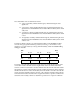
1 Board Level Hardware Description The BusSwitch ASIC provides an interface between the processor bus (MC88110 bus) and the local peripheral bus (MC68040 compatible bus). Refer to the MVME197LE block diagram (Figure 1-1). It provides bus arbitration for the MC88110 bus and serves as a seven level interrupt handler. It has programmable map decoders for both busses, as well as write post buffers on each, two tick timers, and four 32-bit general purpose registers.
Features Features These are some of the major features of the MVME197LE single board computer: ❏ MC88110 RISC Microprocessor ❏ 32 or 64 megabytes of 64-bit Dynamic Random Access Memory (DRAM) with error correction ❏ 1 megabyte of Flash memory ❏ Six status LEDs (FAIL, RUN, SCON, LAN, SCSI, and VME) ❏ 8 kilobytes of Static Random Access Memory (SRAM) and Time of Day (TOD) clock with Battery Backup RAM (BBRAM) ❏ Two push-button switches (ABORT and RESET) ❏ 128 kilobytes of BOOT ROM ❏ Six 32-bit
1 Board Level Hardware Description Specifications The specifications for the MVME197LE are listed in Table 1-1. Table 1-1. MVME197LE Specifications Characteristics Specifications Power requirements +5 Vdc (+/- 2.5%), 4 A (typical), 5 A (maximum) +12 Vdc (+/- 2.5%), 100 mA (maximum) -12 Vdc (+/- 2.
Block Diagram MVME197LEIG/D1 1-5 1
1 Address Address Bus Mezzanine Port 32 Data 64 DCAM MUX Address RAS, CAS PROCESSOR BUS Data Bus ECDM (X4) Data Bus BusSwitch I2CBus Address 32 Data Memory Array 32/64 MB 256 I2C EEPROM 32 LOCAL PERIPHERAL BUS Address Bus Data Bus NVRAM/RTC LAN 82596CA Installation Guide VMEbus (VMEchip2) Flash Memory PCCchip2 SCSI -II NCR53710 Figure 1-1.
Functional Description Functional Description The following sections contain a functional description of the major blocks on the MVME197LE single board computer. Front Panel Switches and Indicators There are two push-button switches and six LEDs on the front panel of the MVME197LE module. The switches are RESET and ABORT. The RESET switch (S3) will reset all onboard devices and drive the SYSRESET* signal if the board is the system controller.
1 Board Level Hardware Description Data Bus Structure The data bus structure is arranged to accommodate the various 8-bit, 16-bit, 32-bit, and 64-bit devices that reside on the module. Refer to the MVME197LE, MVME197DP, and MVME197SP Single Board Computers Programmer’s Reference Guide and to the user’s guide for each device to determine its port size, data bus connection, and any restrictions that apply when accessing the device.
Functional Description DRAM is not disabled by a local peripheral bus reset. Refer to the DCAM and ECDM chapters in the MVME197LE, MVME197DP, and MVME197SP Single Board Computers Programmer’s Reference Guide for detailed programming information. Battery Backup RAM and Clock The MK48T08 RAM and clock chip is used on the MVME197LE. This chip provides a time of day clock, oscillator, crystal, power fail detection, memory write protection, 8KB of RAM, and a battery in one 28-pin package.
1 Board Level Hardware Description operate at synchronous bit rates up to 64k bits per second. It uses RXD, CTS, DCD, RTS, and DTR. It also interfaces to the synchronous clock signal lines. Refer to the MVME197LE, MVME197DP, and MVME197SP Single Board Computers Programmer’s Reference Guide for drawings of the serial port interface connections. All four serial ports use EIA-232-D drivers and receivers located on the main board, and all the signal lines are routed to the I/O connector.
Functional Description The Ethernet Station Address is displayed on a label attached to the VMEbus P2 connector. In addition, the eight bytes including the Ethernet address are stored in the configuration area of the BBRAM, with the two lower bytes of those set to 0. That is, 08003E2XXXXX0000 is stored in the BBRAM. At an address of $FFFC1F2C, the upper four bytes (08003E2X) can be read. At an address of $FFFC1F30, the lower four bytes (XXXX0000) can be read.
1 Board Level Hardware Description Peripheral Resources The MVME197LE includes many resources for the local processor. These include tick timers, software programmable hardware interrupts, watchdog timer, and local peripheral bus timeout. Programmable Tick Timers Six 32-bit programmable tick timers with 1 µsec resolution are provided, two in the BusSwitch, two in the VMEchip2, and two in the PCCchip2. The tick timers can be programmed to generate periodic interrupts to the processor.
Memory Maps µsec, 64 µsec, 256 µsec, or infinite for the local peripheral bus. The local peripheral bus timer does not operate during VMEbus bound cycles. VMEbus bound cycles are timed by the VMEbus access timer and the VMEbus global timer. Interrupt Sources MVME197LE MPU interrupts are channeled through the BusSwitch.
1 Board Level Hardware Description The memory maps of MVME197LE devices are provided in the following tables. Table 1-2 is the entire map from $00000000 to $FFFFFFFF. Many areas of the map are user-programmable, and suggested uses are shown in the table. This is assuming no address translation is used between the processor and local peripheral bus and between the local peripheral bus and VMEbus. The cache inhibit function is programmable in the MC88110.
Memory Maps The following table focuses on the Local Devices portion of the Memory Map. Table 1-3.
1 Board Level Hardware Description 3. Writes to the LCSR in the VMEchip2 must be 32 bits. LCSR writes of 8 or 16 bits terminate with a TEA signal. Writes to the GCSR may be 8, 16, or 32 bits. Reads to the LCSR and GCSR may be 8, 16, or 32 bits. 4. This area does not return an acknowledge signal. If the processor bus timeout timer is enabled, the access times out and is terminated by a TEA signal. 5. Size is approximate. 6.
HARDWARE PREPARATION AND INSTALLATION 2 Introduction This chapter provides unpacking instructions, hardware preparation, and installation instructions for the MVME197LE VMEmodule. The MVME712X transition module hardware preparation is provided in separate manuals, refer to the Related Documentation section of this guide. Unpacking Instructions N ote If shipping carton is damaged upon receipt, request that the carrier’s agent be present during unpacking and inspection of equipment.
Hardware Preparation and Installation 2 2-2 Installation Guide
MVME197LEIG/D1 VMEbus CONNECTOR P1 VMEbus CONNECTOR P2 P1 P2 A1 B1 C1 A32 B32 C32 A1 B1 C1 1A1 1E1 A32 B32 C32 1A17 1A1 2A17 3A1 3A17 1E17 1E1 2E17 3E1 3E17 MEZZANINE CONNECTOR J2 S6 S1 O 1 N 2 3 4 5 6 7 8 O 1 N 2 CONFIGURATION SWITCH S6 SERIAL PORT 4 CLOCK SELECT 9 CONFIGURATION SWITCH S1 GENERAL PURPOSE/SCON MODULE CONNECTOR J1 REMOTE RESET/ABORT/LEDS 20 2 J1 1 DS1 DS2 DS3 DS4 DS5 DS6 FAIL SCON RUN LAN VME SCSI ABORT SWITCH S2 RESET SWITCH S3 S2 S3 Hardw
Hardware Preparation and Installation 2 Configuration Switches The location of the switches, connectors, and LED indicators on the MVME197LE is illustrated in Figure 2-1. The MVME197LE has been factory tested and is shipped with factory switch settings that are described in the following sections. The MVME197LE operates with its required and factoryinstalled Debug Monitor, MVME197Bug (197Bug), with these factory switch setting.
Hardware Preparation Configuration Switch S1: General Purpose Functions (S1-1 to S1-8) The eight General Purpose Input lines (GPI0-GPI7) on the MVME197LE may be configured with selectable switch segments S1-1 through S1-8. These switches can be read as a register (at $FFF40088) in the VMEchip2 LCSR. Refer to the VMEchip2 chapter in the MVME197LE, MVME197DP, and MVME197SP Single Board Computers Programmer’s Reference Guide for the status of lines GPI0 through GPI7.
Hardware Preparation and Installation 2 Configuration Switch S6: Serial Port 4 Clock Select (S6-1, S6-2) Serial port 4 can be configured to use clock signals provided by the RTXC4 and TRXC4 signal lines. Switch segments S6-1 and S6-2 on the MVME197LE configures serial port 4 to drive or receive TRXC4 and RTXC4, respectively. Factory configuration is with serial port 4 set to receive both signals (open).
Installation Instructions MVME197LE Module Installation 2 Now that the MVME197LE module is ready for installation, proceed as follows: a. Turn all equipment power OFF and disconnect the power cable from the power source. C aution ! WARNING Inserting or removing modules while power is applied could result in damage to module components. DANGEROUS VOLTAGES, CAPABLE OF CAUSING DEATH, ARE PRESENT IN THIS EQUIPMENT. USE EXTREME CAUTION WHEN HANDLING, TESTING, AND ADJUSTING. b.
Hardware Preparation and Installation provided in the MVME197LE, MVME197DP, and MVME197SP Single Board Computers Programmer’s Reference Guide). Some cable(s) are not provided with the MVME712X module and therefore, are made or provided by the user. (Motorola recommends using shielded cables for all connections to peripherals to minimize radiation). Connect the peripherals to the cable(s). 2 g. Install any other required VMEmodules in the system. h. Replace the chassis cover. i.
Installation Instructions Multiple MVME197LE modules may be configured into a single VME card cage. In general, hardware multiprocessor features are supported. 2 Other MPUs on the VMEbus can interrupt, disable, communicate with and determine the operational status of the RISC processor(s). One register of the GCSR set includes four bits which function as location monitors to allow one MVME197LE processor to broadcast a signal to other MVME197LE processors, if any.
Hardware Preparation and Installation 2 2-10 Installation Guide
DEBUGGER GENERAL INFORMATION 3 Overview of M88000 Firmware The firmware for the M88000-based (88K) series of board and system level products has a common genealogy, deriving from the BUG firmware currently used on all Motorola M68000-based (68K) CPU modules. The M88000 firmware family provides a high degree of functionality and user friendliness, and yet stresses portability and ease of maintenance.
Debugger General Information the diagnostic prompt “197-Diag>” is displayed and the user has all of the diagnostic commands at his disposal as well as all of the debugger commands. The user may switch between directories by using the Switch Directories (SD) command, or may examine the commands in the particular directory that the user is currently in by using the Help (HE) command. 3 Because 197Bug is command-driven, it performs its various operations in response to user commands entered at the keyboard.
Installation and Start-up C aution Inserting or removing modules while power is applied could damage module components. 1. Turn all equipment power OFF. Refer to the Hardware Preparation and Installation chapter in this manual for selecting the configuration switch settings required for the user’s particular application. 2. Refer to the set-up procedure for the user’s particular chassis or system for details concerning the installation of the MVME197LE. 3.
Debugger General Information Note that the MVME197LE also contains a parallel port. To use a parallel device, such as a printer, with the MVME197LE, connect it to the “printer” port at P2 through an MVME712X transition module. Refer to the MVME197LE, MVME197DP, and MVME197SP Single Board Computers Programmer’s Reference Guide for some possible connection diagrams. However, you could also use a module such as the MVME335 for a parallel port connection. 3 5. Power up the system.
ROMboot C aution Although streaming tape can be used to autoboot, the same power supply must be connected to the streaming tape drive, controller, and the MVME197LE. At power-up, the tape controller will position the streaming tape to load point where the volume ID can correctly be read and used.
Debugger General Information automatically scans for controllers and devices in a specified sequence until a valid bootable device containing a boot media is found or the list is exhausted. If a valid bootable device is found, a boot from that device is started. The controller scanning sequence goes from the lowest controller Logical Unit Number (LUN) detected to the highest LUN detected. (Refer to Appendix C for default LUNs).
Restarting the System just been powered up. All static variables (including disk device and controller parameters) are restored to their default states. The breakpoint table and offset registers are cleared. The target registers are invalidated. Input and output character queues are cleared. Onboard devices (timer, serial ports, etc.) are reset, and the first two serial ports are reconfigured to their default state.
Debugger General Information SYSFAIL* Assertion/Negation Upon a reset/power up condition the debugger asserts the VMEbus SYSFAIL* line (refer to the VMEbus specification).
Memory Requirements Terminal Input/Output Control When entering a command at the prompt, the following control codes may be entered for limited command line editing. N ote 3 The presence of the upward caret, “^”, before a character indicates that the Control (CTRL) key must be held down while striking the character key. ^X (cancel line) The cursor is backspaced to the beginning of the line.
Debugger General Information Disk I/O Support 197Bug can initiate disk input/output by communicating with intelligent disk controller modules over the VMEbus. Disk support facilities built into 197Bug consist of command-level disk operations, disk I/O system calls (only via one of the TRAP #496 instructions) for use by user programs, and defined data structures for disk parameters.
Disk I/O Support made, the next time a probe is done it simply returns with “device present” status (pointer to the device descriptor). Disk I/O via 197Bug Commands These following 197Bug commands are provided for disk I/O. Detailed instructions for their use are found in the MVME197BUG 197Bug Debugging Package User’s Manual.
Debugger General Information Disk I/O via 197Bug System Calls All operations that actually access the disk are done directly or indirectly by 197Bug TRAP #496 system calls. (The command-level disk operations provide a convenient way of using these system calls without writing and executing a program). 3 The following system calls are provided to allow user programs to do disk I/O: .DSKRD Disk read. System call to read blocks from a disk into memory. .DSKWR Disk write.
Disk I/O Support Default 197Bug Controller and Device Parameters 197Bug initializes the parameter tables for a default configuration of controllers and devices (refer to Appendix B). If the system needs to be configured differently than this default configuration (for example, to use a 70MB Winchester drive where the default is a 40MB Winchester drive), then these tables must be changed. There are three ways to change the parameter tables: ❏ Using BO or BH.
Debugger General Information Physical Layer Manager Ethernet Driver This driver manages/surrounds the Ethernet controller chip or board. Management is in the scope of the reception of packets, the transmission of packets, receive buffer flushing, and interface initialization. 3 This module ensures that the packaging and unpackaging of Ethernet packets is done correctly in the Boot PROM.
Multiprocessor Support Network Boot Control Module The “control” capability of the Network Boot Control Module is needed to tie together all the necessary modules (capabilities) and to sequence the booting process. The booting sequence consists of two phases: the first phase is labeled “address determination and bootfile selection” and the second phase is labeled “file transfer”. The first phase will utilize the RARP/BOOTP capability and the second phase will utilize the TFTP capability.
Debugger General Information The status codes that may be set by the bus master are: 3 ASCII G (HEX 47) Use Go Direct (GD) logic specifying the MPAR address. ASCII B (HEX 42) Install breakpoints using the Go (G) logic. The Multiprocessor Address Register (MPAR), located in shared RAM location of $3004 offset from the base address the debugger loads it at, contains the second of two words used to control communication between processors.
Diagnostic Facilities GCSR Method A remote processor can initiate program execution in the local MVME197LE dual-port RAM by issuing a remote GO command using the VMEchip2 Global Control and Status Register (GCSR). The remote processor places the MVME197LE execution address in general purpose registers 0 and 1 (GPCSR0 and GPCSR1). The remote processor then sets bit 8 (SIG0) of the VMEchip2 LM/SIG register. This causes the MVME197LE to install breakpoints and begin execution.
Debugger General Information 3 3-18 Installation Guide
USING THE 197Bug DEBUGGER 4 Entering Debugger Command Lines 197Bug is command-driven and performs its various operations in response to user commands entered at the keyboard. When the debugger prompt (197Bug>) appears on the terminal screen, then the debugger is ready to accept commands. As the command line is entered, it is stored in an internal buffer.
Using the 197Bug Debugger The commands are shown using a modified Backus-Naur form syntax. The meta symbols used are: boldface strings A boldface string is a literal such as a command or a program name, and is to be typed just as it appears. italic strings An italic string is a “syntactic variable” and is to be replaced by one of a class of items it represents.
Entering Debugger Command Lines Data Type Base Identifier Examples Integer Hexadecimal $ $FFFFFFFF Integer Decimal & &1974, &10-&4 Integer Octal @ @456 Integer Binary % %1000110 4 If no base identifier is specified, then the numeric value is assumed to be hexadecimal. A numeric value may also be expressed as a string literal of up to four characters. The string literal must begin and end with the single quote mark (’).
Using the 197Bug Debugger Address as a Parameter Many commands use ADDR as a parameter. The syntax accepted by 197Bug is similar to the one accepted by the one-line assembler. All control addressing modes are allowed. An “address + offset register” mode is also provided. Address Formats Addresses are entered as a hexadecimal number, e.g., 20000 would correspond to address $00020000.
Entering and Debugging Programs N ote Relative addresses are limited to 1MB (5 digits), regardless of the range of the closest offset register. Port Numbers Some 197Bug commands give the user the option to choose the port to be used to input or output. Valid port numbers which may be used for these commands are: N ote 1. MVME197LE EIA-232-D Debug (Terminal Port 0 or 00) (PORT 1 on the MVME197LE P2 connector).
Using the 197Bug Debugger Other ways are by reading in the program from disk, using one of the disk commands (BO, BH, IOP), or by reading the program as a file from a remote computer on a network, using one of the network commands, such as NIOP. Once the object code has been loaded into memory, the user can set breakpoints if desired and run the code or trace through it.
Floating Point Support CPU/MPU Registers MPU register CR20 is reserved for usage by the debugger. If CR20 is to be used by the user program, it must be restored prior to utilizing debugger resources (system calls). Floating Point Support The floating point Special Function Unit (SFU) of the MC88110 microprocessor chip is supported in this version of 197Bug.
Using the 197Bug Debugger Single Precision Real This format would appear in memory as: 4 1-bit sign field (1 binary digit) 8-bit biased exponent field (2 hex digits. Bias = $7F) 23-bit fraction field (6 hex digits) A single precision number takes 4 bytes in memory. Double Precision Real This format would appear in memory as: 1-bit sign field (1 binary digit) 11-bit biased exponent field (3 hex digits.
197Bug Debugger Command Set 197Bug Debugger Command Set The 197Bug debugger commands are summarized in Table 4-1. The command syntax is shown using the symbols explained earlier in this chapter. The CNFG and ENV commands are explained in Appendix A. Controllers, devices, and their LUNs are listed in Appendix B. All other command details are explained in the MVME197BUG 197Bug Debugging Package User’s Manual. Table 4-1.
Using the 197Bug Debugger Table 4-1.
197Bug Debugger Command Set Table 4-1.
Using the 197Bug Debugger Table 4-1.
197Bug Debugger Command Set Table 4-1.
Using the 197Bug Debugger 4 4-14 Installation Guide
CONFIGURE AND ENVIRONMENT COMMANDS A Configure Board Information Block CNFG [;[M][I]] This command is used to display and configure the board information block. This block is resident within the Non-Volatile RAM (NVRAM). Refer to the MVME197LE Single Board Computer User’s Manual for the actual location. The board information block contains various elements detailing specific operation parameters of the hardware.
A Configure and Environment Commands Modification is permitted by using the M option of the command. At the end of the modification session, you are prompted for the update to Non-Volatile RAM (NVRAM). A Y response must be made for the update to occur; any other response terminates the update (disregards all changes). The update also recalculates the checksum. Take caution when modifying parameters.
Set Environment to Bug/Operating System Table A-1. ENV Command Parameters ENV Parameter and Options Default Meaning of Default Bug or System Environment [B/S] B Bug is the standard mode of operation. Field Service Menu Enable [Y/N] N Do no display the field service menu.
A Configure and Environment Commands Table A-1. ENV Command Parameters (Continued) ENV Parameter and Options Default Meaning of Default Auto Boot at power-up only [Y/N] Y Auto Boot is attempted at power-up reset only. Auto Boot Controller LUN 00 LUN of a disk/tape controller module currently supported by the Bug. The default is $0. Auto Boot Device LUN 00 LUN of a disk/tape device currently supported by the Bug. The default is $0.
Set Environment to Bug/Operating System Table A-1. ENV Command Parameters (Continued) ENV Parameter and Options Default Meaning of Default ROM Boot Abort Delay 0 Time in seconds that the ROMboot sequence will delay before starting. The purpose is to allow the user the option of stopping the boot by use of the Break key. The time value is from 0 through 255 seconds. ROM Boot Direct Starting Address FF800000 First location tested when the Bug searches for a ROMboot Module.
A Configure and Environment Commands Table A-1. ENV Command Parameters (Continued) ENV Parameter and Options Default Meaning of Default Network Auto Boot Device LUN 00 LUN of a disk/tape device currently supported by the Bug. Default is $0. Network Auto Boot Configuration Parameter Pointer (NVRAM) 00000000 This is the address where the network interface configuration parameters are to be saved/retained in NVRAM: these parameters are the necessary parameters to perform an unattended network boot.
Set Environment to Bug/Operating System Table A-1. ENV Command Parameters (Continued) ENV Parameter and Options Default Meaning of Default Memory Search Delay Address FFFFD00F The default address is $FFFFD00F. This is the MVME197LE GCSR (global control and status register) GPCSR5 as accessed through the VMEbus A16 space and assumes that the MVME197LE GRPAD (group address) and BDAD (board address within group) switches are set to “ON”.
A Configure and Environment Commands Table A-1. ENV Command Parameters (Continued) ENV Parameter and Options Default Memory Size Ending Address 02000000 Base Address of Local Memory 00000000 Size of Local Memory 02000000 Meaning of Default The default ending address is the calculated size of local memory. The beginning address of Local Memory. It must be a multiple of the Local Memory board size, starting with 0.
Set Environment to Bug/Operating System Table A-1. ENV Command Parameters (Continued) ENV Parameter and Options Default Meaning of Default Slave Address Translation Address #1 00000000 This register will allow the VMEbus address and the local address to be different. The value in this register is the base address of the local resource that is associated with the starting and ending address selections from the previous questions. The default is 0.
A Configure and Environment Commands Table A-1. ENV Command Parameters (Continued) ENV Parameter and Options Default Meaning of Default Slave Address Translation Address #2 00000000 This register will allow the VMEbus address and the local address to be different. The value in this register is the base address of the local resource that is associated with the starting and ending address selections from the previous questions. The default is 0.
Set Environment to Bug/Operating System Table A-1. ENV Command Parameters (Continued) ENV Parameter and Options Default Meaning of Default Master Control #1 0D This defines the access characteristics for the address space defined with this master address decoder. Master Enable #2 [Y/N] Y Set up and enable the Master Address Decoder #2. Master Starting Address #2 FF000000 This is the base address of the VMEbus resource that is accessible from the local peripheral bus.
A Configure and Environment Commands Table A-1. ENV Command Parameters (Continued) ENV Parameter and Options Default Meaning of Default Master Starting Address #3 00000000 Base address of the VMEbus resource that is accessible from the local peripheral bus. If enabled, the value is calculated as 1 less than the calculated size of memory. If not enabled, default is $00000000. Master Ending Address #3 00000000 Ending address of the VMEbus resource that is accessible from the local peripheral bus.
Set Environment to Bug/Operating System Table A-1. ENV Command Parameters (Continued) ENV Parameter and Options Default Meaning of Default Master Address Translation Address #4 00000000 This register will allow the VMEbus address and the local address to be different. The value in this register is the base address of VMEbus resource that is associated with the starting and ending address selections from the previous questions. The default is 0.
A Configure and Environment Commands Table A-1. ENV Command Parameters (Continued) ENV Parameter and Options Default Meaning of Default F-Page (VMEbus A24) Control 02 This defines the access characteristics for the address space defined with the F-Page address decoder. Default is $02. ROM Speed Bank A Code ROM Speed Bank B Code 03 03 These parameters are used to set up the ROM speed. Default $03 = 165 nsec.
DISK/TAPE CONTROLLER DATA B Disk/Tape Controller Modules Supported The following VMEbus disk/tape controller modules are supported by the 197Bug. The default address for each type of controller is the First Address and the controller can be addressed by the First CLUN during commands BH, BO, or IOP, or during TRAP #496 calls .DSKRD or .DSKWR.
Disk/Tape Controller Data B Disk/Tape Controller Default Configurations Single Board Computers - 7 Devices Controller LUN Address Device LUN Device Type 0 $XXXXXXXX 00 10 20 30 40 50 60 SCSI Common Command Set (CCS), which may be any of these: - Fixed direct access device - Removable flexible direct access (TEAC style) - CD-ROM - Sequential access device MVME320 - 4 Devices Controller LUN Address Device LUN 11 $FFFFB000 12 $FFFFAC00 0 1 2 3 Device Type Winchester hard drive Winchester hard
Disk/Tape Controller Default Configurations MVME327A - 9 Devices B Controller LUN Address Device LUN Device Type 2 $FFFFA600 SCSI Common Command Set (CCS), which may be any of these: 3 $FFFFA700 00 10 20 30 40 50 60 80 81 Local Floppy Drive Local Floppy Drive - Fixed direct access device - Removable flexible direct access (TEAC style) - CD-ROM - Sequential access device MVME328 - 14 Devices Controller LUN Address Device LUN Device Type 6 $FFFF9000 SCSI Common Command Set (CCS), which m
Disk/Tape Controller Data MVME350 - 1 Device B B-4 Controller LUN Address Device LUN 4 $FFFF5000 0 5 $FFFF5100 Device Type QIC-02 Streaming Tape Drive Installation Guide
IOT Command Parameters for Supported Floppy Types IOT Command Parameters for Supported Floppy Types The following table lists the proper IOT command parameters for floppies used with boards such as the MVME328 and MVME197LE. Floppy Types and Formats IOT Parameter Sector Size: 0- 128 1- 256 2- 512 3-1024 4-2048 5-4096 = Block Size: 0- 128 1- 256 2- 512 3-1024 4-2048 5-4096 = Sectors/Track Number of Heads = Number of Cylinders = Precomp.
Disk/Tape Controller Data B B-6 Installation Guide
NETWORK CONTROLLER DATA C Network Controller Modules Supported The following VMEbus network controller modules are supported by the MVME197Bug. The default address for each type and position is showed to indicate where the controller must reside to be supported by the MVME197Bug. The controllers are accessed via the specified CLUN and DLUNs listed here.
Network Controller Data C C-2 Installation Guide
Index When using this index, keep in mind that a page number indicates only where referenced material begins. It may extend to the page or pages following the page referenced.
Index connector P2 4-5 connectors, P1 and P2 1-12 console port 4-5 Control (CTRL) key 3-9 controller B-1 controller parameters, default 3-13 controllers supported B-1, C-1 count 4-2 CPU register 4-4 CPU/MPU registers 4-7 D I N D E X Data Bus Structure 1-7 debugger commands 4-9 debugger directory 3-17 debugger prompt 3-1, 4-1 debugging programs 4-5 default 197Bug controller and device parameters 3-13 default baud rate 3-3 delimiter 4-2 description of 197Bug 3-1 device descriptor table 3-10 device paramet
Global Control and Status Register (GCSR) 3-17 H handshaking 3-3 hard disk drive B-2 hardware functions 4-6 hardware interrupt, VMEchip2 1-11 Help (HE) command 3-2 host port 4-5 I I/O control, terminal 3-9 I/O disk - error codes 3-13 I/O error codes, network 3-15 I/O Interfaces 1-8 I/O support, disk 3-10 I/O support, network 3-13 I/O, disk - 197Bug commands 3-11 I/O, disk - system calls 3-12 implementation of 197Bug 3-2 inquiry 3-10 installation 3-2 installation and start-up 3-2 Installation Instructions
Index Multiprocessor Control Register (MPCR) method 3-15 multiprocessor support 3-15 MVME197BUG 3-1 MVME197LE Block Diagram 1-5 MVME197LE Module Installation 2-6 MVME197LE registers 2-1 MVME197LE Specifications 1-4 MVME320 B-2 MVME323 B-2 MVME327A B-3 MVME328 B-3 MVME350 B-4 MVME376 C-1 MVME712M Transition Module and P2 Adapter Board User’s Manual 2-5 MVME712X 1-1 MVME712-XX 1-1 N negation, SYSFAIL* 3-8 network boot control module 3-15 network controllers supported C-1 network I/O error codes 3-15 network
SCSI Interface 1-10 SCSI Termination 1-10 sector 3-10 sectors versus blocks 3-10 Sequential access device B-2, B-3 SERIAL PORT 1 4-5 SERIAL PORT 2 4-5 Serial Port Interface 1-8 Set Environment to Bug/Operating System A-2 sign field 4-7 Single Board Computers B-2 single precision real 4-8 Software-Programmable Hardware Interrupts 1-11 source line 4-5 Special Function Unit (SFU) 4-7 specifications, MVME197LE 1-4 square brackets 4-2 start-up 3-2 static variable space 3-8 Storage temperature 1-4 string literal
Index I N D E X IN-6 Installation Guide