
Laptop User Manual

Programming Model
http://www.motorola.com/computer/literature 3-41
3
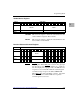
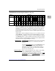
SDRAM Enable and Size Register (Blocks A, B, C, D)
Writes to this register must be enveloped by a period of time in which no
accesses to SDRAM occur. The requirements of the envelope are that all
SDRAM accesses must have completed before the write starts and none
should begin until after the write is done. A simple way to do this is to
perform at least two read accesses to this (or another register) before and
after the write.
Additionally, sometime during the envelope, before or after the write, all
of the SDRAMs’ open pages must be closed and the Hawk’s open page
tracker must be reset. The way to do this is to allow enough time for at least
one SDRAM refresh to occur by waiting for the 32-bit counter (see register
description further on in this chapter) to increment at least 100 times. The
wait period needs to happen during the envelope.
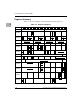
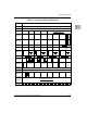
ram a/b/c/d en
ram a/b/c/d en enables 60x accesses to the corresponding
block of SDRAM when set, and disables them when
cleared.
Note that ram e/f/g/h en
are located at $FEF800C0 (refer
to the section on SDRAM Enable and Size Register
(Blocks E, F, G, H) further on in this chapter for more
information.) They operate the same for blocks E-H as
these bits do for blocks A-D.
ram a/b/c/d siz0-3
These control bits define the size of their corresponding
block of SDRAM. Table 3-10 shows the block
configuration assumed by the SMC for each value of ram
siz0-ram siz3. Note that ram e/f/g/h size0-3 are located
at $FEF800C0. They operate identically for blocks E-H as
these bits do for blocks A-D.
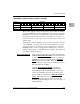
Address
$FEF80010
Bit
0
1
2
3
4
5
6
7
8
9
10
11
12
13
14
15
16
17
18
19
20
21
22
23
24
25
26
27
28
29
30
31
Name
ram a en
0
0
0
ram a siz0
ram a siz1
ram a siz2
ram a siz3
ram b en
0
0
0
ram b siz0
ram b siz1
ram b siz2
ram b siz3
ram c en
0
0
0
ram c siz0
ram c siz1
ram c siz2
ram c siz3
ram d en
0
0
0
ram d siz0
ram d siz1
ram d siz2
ram d siz3
Operation
R/W
R
R
R
R/W
R/W
R/W
R/W
R/W
R
R
R
R/W
R/W
R/W
R/W
R/W
R
R
R
R/W
R/W
R/W
R/W
R/W
R
R
R
R/W
R/W
R/W
R/W
Reset
0 PL
X
X
X
0 P
0 P
0 P
0 P
0 PL
X
X
X
0 P
0 P
0 P
0 P
0 PL
X
X
X
0 P
0 P
0 P
0 P
0 PL
X
X
X
0 P
0 P
0 P
0 P