
Personal Computer User Manual


Connectors
http://www.motorola.com/computer/literature 5-23
5
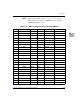
VMEbus Connectors P1 & P2 Pin Assignments (PMC mode)
The VMEbus connector P1 provides power and VME signals for 24-bit
address and 16-bit data. The pin assignments for the connector are
specified by the IEEE P1014-1987 VMEbus Specification and the VME64
Extension Standard.
Row B of connector P2 provides power to the MVME5100, and to the
upper eight VMEbus address lines, and additional 16 VMEbus data lines.
Rows A, C, Z, and D provide power and interface signals to the
MVME762 transition module. The pin assignments for connector P2 in
PMC mode are as follows:
Table 5-13. VMEbus Connector P2 Pin Assignments
(PMC Mode)
Pin Row Z Row A Row B Row C Row D
1
PMC2_2 (J24-2) PMC1_2 (J14-2) +5V PMC1_1 (J14-1) PMC2_1 (J24-1)
2
GND PMC1_4 (J14-4) GND PMC1_3 (J14-3) PMC2_3 (J24-3)
3
PMC2_5 (J24-5) PMC1_6 (J14-6) RETRY# PMC1_5 (J14-5) PMC2_4 (J24-4)
4
GND PMC1_8 (J14-8) VA24 PMC1_7 (J14-7) PMC2_6 (J24-6)
5
PMC2_8 (J24-8) PMC1_10 (J14-10) VA25 PMC1_9 (J14-9) PMC2_7 (J24-7)
6
GND PMC1_12 (J14-12) VA26 PMC1_11 (J14-11) PMC2_9 (J24-9)
7
PMC2_11(J24-11) PMC1_14 (J14-14) VA27 PMC1_13 (J14-13) PMC2_10 (J24-10)
8
GND PMC1_16 (J14-16) VA28 PMC1_15 (J14-15) PMC2_12 (J24-12)
9
PMC2_14 (J24-14) PMC1_18 (J14-18) VA29 PMC1_17 (J14-17) PMC2_13 (J24-13)
10
GND PMC1_20 (J14-20) VA30 PMC1_19 (J14-19) PMC2_15 (J24-15)
11
PMC2_17 (J24-17) PMC1_22 (J14-22) VA31 PMC1_21 (J14-21) PMC2_16 (J24-16)
12
GND PMC1_24 (J14-24) GND PMC1_23 (J14-23) PMC2_18 (J24-18)
13
PMC2_20 (J24-20) PMC1_26 (J14-26) +5V PMC1_25 (J14-25) PMC2_19 (J24-19)