
Personal Computer User Manual


Connectors
http://www.motorola.com/computer/literature 5-25
5
VMEbus P1 & P2 Connector Pin Assignments (SBC Mode)
The VMEbus connector P1 provides power and VME signals for 24-bit
address and 16-bit data. The pin assignments for the connector are
specified by the IEEE P1014-1987 VMEbus Specification and the VME64
Extension Standard.
Row B of connector P2 provides power to the MVME5100 and to the
upper 8 VMEbus address lines and additional 16 VMEbus data lines.
Rows A, C, Z, and D provide power and interface signals to the
MVME712 or MVME761 transition module in SBC mode (also called 761
mode and IPMC mode).
It is important to note that the PMC I/O routing to row D and Z are not the
same as MVME2600/2700. The PMC I/O routing for row D and row Z is
the same as the PMC mode with the exception of pins Z1, 3, 5, 7, 9, 11, 13,
15, and 17 which are used for extended SCSI.
Note A PMC card installed in slot 2 of an MVME5100 in SBC
mode MUST NOT connect to J24-2, 5, 8, 11, 14, 17, 20, 23,
and 26 since they are connected to the extended SCSI signals
of the MVME5100.
The pin assignments for the P2 connector using the IPMC761 or the
IPMC712 are listed in the following two tables:
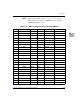
Table 5-14. VMEbus P2 Connector Pinouts with IPMC761-
SBC Mode
Pin Row Z Row A Row B Row C Row D
1 DB8# DB0# +5V RD- (10/100) PMC2_1 (J24-1)
2 GND DB1# GND RD+ (10/100) PMC2_3 (J24-3)
3 DB9# DB2# RETRY# TD- (10/100) PMC2_4 (J24-4)
4 GND DB3# VA24 TD+ (10/100) PMC2_6 (J24-6)
5 DB10# DB4# VA25 Not Used PMC2_7 (J24-7)
6 GND DB5# VA26 Not Used PMC2_9 (J24-9)