
Personal Computer User Manual


6-2 Computer Group Literature Center Web Site
Programming the MVME51xx
6
Processor Bus Memory Map
The processor memory map configuration is under the control of the PHB
and SMC portions of the Hawk ASIC. The Hawk adjusts system mapping
to suit a given application via programmable map decoder registers. At
system power-up or reset, a default processor memory map takes over.
Default Processor Memory Map
The default processor memory map that is valid at power-up or reset
remains in effect until reprogrammed for specific applications. Table 6-1
defines the entire default map ($00000000 to $FFFFFFFF).
Note The first 1MB of ROM/FLASH Bank A (soldered Flash up
to 8MB) appears in this range after a reset if the rom_b_rv
control bit in the SMC’s ROM B Base/Size register is
cleared. If the rom_b_rv control bit is set, this address range
maps to ROM/FLASH Bank B (socketed 1MB Flash).
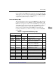
Table 6-1. Default Processor Memory Map
Processor Address
Size Definition
Start End
0000 0000 7FFF FFFF 2GB Not Mapped
8000 0000 8080 FFFF 8M+64K Zero-based PCI/ISA I/O Space
8081 0000 FEF7 FFFF 2GB-24MB-576KB Not Mapped
FEF8 0000 FEF8 FFFF 64KB System Memory Controller Registers
FEF9 0000 FEFE FFFF 384KB Not Mapped
FEFF 0000 FEFF FFFF 64KB PCI Host Bridge (PHB) Registers
FF00 0000 FFEF FFFF 15MB Not Mapped
FFF0 0000 FFFF FFFF 1MB ROM/FLASH Bank A or Bank B (See
Note)