
Personal Computer User Manual


Memory Maps
http://www.motorola.com/computer/literature 6-3
6
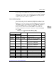
For an example of the CHRP memory map, refer to the following table. For
detailed processor memory maps, including suggested CHRP- and PREP-
compatible memory maps, refer to the MVME5100-Series Single Board
Computer Programmer’s Reference Guide.
Processor Memory Map
The following table describes a suggested CHRP Memory Map from the
point of view of the processor. This memory map is an alternative to the
PREP memory map. Note: in all recommended CHRP maps, the beginning
of PCI Memory Space is determined by the end of DRAM rounded up to
the nearest 256MB-boundry as required by CHRP. For example, if
memory was 1G on the baseboard and 192MB on a mezzanine, the
beginning of PCI memory would be rounded up to address 0x50000000
(1G + 256M).
Table 6-2. Suggested CHRP Memory Map
Processor Address Size Definition Notes
Start End
0000 0000 top_dram dram_size System Memory (onboard DRAM) 1
top_dram 8000 0000 variable PCI Memory Space 1, 5
8100 0000 9FFF FFFF 512MB A32/D32 space mapped to VMEbus
starting address of 0100 0000
A000 0000 A1FF FFFF 32MB A24/D16 space mapped to VMEbus
starting address of F000 0000
AFFF 0000 AFFF FFFF 64KB A16/D16 space mapped to VMEbus
starting address of FFFF 0000
F400 0000 F7FF FFFF 64MB FLASH Bank A (optional) 1, 2
F800 0000 FBFF FFFF 64MB FLASH Bank B (optional) 1, 2
FC00 0000 FDFF FFFF 32MB Reserved
FE00 0000 FE7F FFFF 8MB PCI/ISA I/O Space 1
FE80 0000 FEF7 FFFF 7.5MB Reserved
FEF8 0000 FEF8 FFFF 64KB System Memory Controller Registers
FEF9 0000 FEFE FFFF 384KB Reserved
FEFF 0000 FEFF FFFF 64KB Processor Host Bridge Registers 4