
Personal Computer User Manual


6-4 Computer Group Literature Center Web Site
Programming the MVME51xx
6
Notes
1. Programmable via Hawk ASIC.
2. The actual Power Plus II size of each ROM/FLASH bank may vary.
3. The first 1MB of ROM/FLASH Bank A appears at this range after
a reset if the rom_b_rv control bit is cleared. If the rom_b_rv control
bit is set, this address maps to ROM/FLASH Bank B.
4. The only method to generate a PCI Interrupt Acknowledge cycle
(8259 IACK) is to perform a read access to the Hawks PIACK
Register at 0xFEFF0030.
5. VME should be placed at the top of PCI memory space.
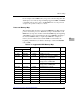
The following table shows the programmed values for the associated
Hawk PCI Host Bridge Registers for the suggested Processor Memory
Map.
FF00 0000 FF7F FFFF 8MB FLASH Bank A (preferred) 1, 2
FF80 0000 FF8F FFFF 1MB FLASH Bank B (preferred) 1, 2
FF90 0000 FFEF FFFF 6MB Reserved
FFF0 0000 FFFF FFFF 1MB Boot ROM 3
Table 6-3. Hawk PPC Register Values for Suggested Memory
Map
Address Register Name Register Name
FEFF 0040 MSADD0 X000 F3FF [X:1..8]
FEFF 0044 MSOFF0 & MSATT0 0000 00C2
FEFF 0048 MSADD1 FE00 FE7F
FEFF 004C MSOFF1 & MSATT1 0200 00C0
Table 6-2. Suggested CHRP Memory Map (Continued)
Processor Address Size Definition Notes
Start End