SPRS292A − OCTOBER 2005 − REVISED NOVEMBER 2005 D Excellent-Price/Performance Floating-Point D D D D D Digital Signal Processor (DSP): TMS320C6711D − Eight 32-Bit Instructions/Cycle − 167-, 200-, 250-MHz Clock Rates − 6-, 5-, 4-ns Instruction Cycle Time − 1000, 1200, 1500 MFLOPS Advanced Very Long Instruction Word (VLIW) C67x DSP Core − Eight Highly Independent Functional Units: − Four ALUs (Floating- and Fixed-Point) − Two ALUs (Fixed-Point) − Two Multipli
SPRS292A − OCTOBER 2005 − REVISED NOVEMBER 2005 Table of Contents revision history . . . . . . . . . . . . . . . . . . . . . . . . . . . . . . . . . . . . . . 3 GDP and ZDP BGA packages (bottom view) . . . . . . . . . . . . 4 description . . . . . . . . . . . . . . . . . . . . . . . . . . . . . . . . . . . . . . . . . 5 device characteristics . . . . . . . . . . . . . . . . . . . . . . . . . . . . . . . . 6 device compatibility . . . . . . . . . . . . . . . . . .
SPRS292A − OCTOBER 2005 − REVISED NOVEMBER 2005 REVISION HISTORY The TMS320C6711D device-specific documentation has been split from TMS320C6711, TMS320C6711B, TMS320C6711C, TMS320C6711D Floating−Point Digital Signal Processors, literature number SPRS088N, into a separate Data Sheet, literature number SPRS292. It also highlights technical changes made to SPRS292 to generate SPRS292A; these changes are marked by “[Revision A]” in the Revision History table below.
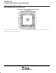
SPRS292A − OCTOBER 2005 − REVISED NOVEMBER 2005 GDP and ZDP BGA packages (bottom view) GDP and ZDP 272-PIN BALL GRID ARRAY (BGA) PACKAGES† ( BOTTOM VIEW ) Y W V U T R P N M L K J H G F E D C B A 3 5 7 9 11 13 15 17 19 2 4 6 8 10 12 14 16 18 20 † The ZDP mechanical package designator represents the version of the GDP package with lead−free balls. For more detailed information, see the Mechanical Data section of this document.
SPRS292A − OCTOBER 2005 − REVISED NOVEMBER 2005 description The TMS320C67x DSPs (including the TMS320C6711, TMS320C6711B, TMS320C6711C, TMS320C6711D devices†) compose the floating-point DSP family in the TMS320C6000 DSP platform.
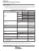
SPRS292A − OCTOBER 2005 − REVISED NOVEMBER 2005 device characteristics Table 1 provides an overview of the C6711D DSP. The table shows significant features of the device, including the capacity of on-chip RAM, the peripherals, the execution time, and the package type with pin count. For more details on the C6000 DSP device part numbers and part numbering, see Figure 5. Table 1.
SPRS292A − OCTOBER 2005 − REVISED NOVEMBER 2005 device compatibility The TMS320C6211/C6211B and C6711/C6711B devices are pin-compatible and have the same peripheral set; thus, making new system designs easier and providing faster time to market.
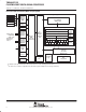
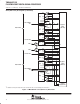
SPRS292A − OCTOBER 2005 − REVISED NOVEMBER 2005 functional block and CPU (DSP core) diagram SDRAM SBSRAM 32 SRAM External Memory Interface (EMIF) ROM/FLASH Timer 0 I/O Devices Timer 1 Multichannel Buffered Serial Port 1 (McBSP1) Framing Chips: H.
SPRS292A − OCTOBER 2005 − REVISED NOVEMBER 2005 CPU (DSP core) description The CPU fetches advanced very-long instruction words (VLIW) (256 bits wide) to supply up to eight 32-bit instructions to the eight functional units during every clock cycle. The VLIW architecture features controls by which all eight units do not have to be supplied with instructions if they are not ready to execute.
SPRS292A − OCTOBER 2005 − REVISED NOVEMBER 2005 CPU (DSP core) description (continued) ÁÁÁÁÁÁÁÁ ÁÁÁÁÁÁÁ ÁÁÁÁÁÁÁÁ ÁÁÁÁÁÁÁ ÁÁÁÁÁÁ ÁÁÁÁÁÁ ÁÁÁÁÁÁ ÁÁÁÁÁÁ ÁÁÁÁÁ ÁÁÁÁÁÁÁÁ ÁÁÁÁÁÁÁÁ ÁÁÁÁÁÁ ÁÁÁÁÁÁÁÁ ÁÁÁÁÁÁÁÁ ÁÁÁÁÁ ÁÁÁÁÁÁ ÁÁÁÁÁÁ ÁÁÁÁÁÁ ÁÁÁÁÁÁ ÁÁÁÁÁ ÁÁÁÁÁÁÁÁ ÁÁÁÁÁÁÁÁ ÁÁÁÁÁÁ ÁÁÁÁÁÁÁÁ ÁÁÁÁÁÁÁÁ ÁÁÁÁÁ ÁÁÁÁÁÁ ÁÁÁÁÁÁ ÁÁÁÁÁ ÁÁÁÁÁ ÁÁÁÁÁÁÁ ÁÁÁÁÁÁÁÁ ÁÁÁÁÁÁÁÁ ÁÁÁÁÁÁÁÁ src1 .L1† src2 dst long dst long src LD1 32 MSB ST1 8 8 long src long dst dst .
SPRS292A − OCTOBER 2005 − REVISED NOVEMBER 2005 memory map summary Table 2 shows the memory map address ranges of the device. Internal memory is always located at address 0 and can be used as both program and data memory. The configuration registers for the common peripherals are located at the same hex address ranges. The external memory address ranges in the device begin at the address location 0x8000 0000. Table 2.
SPRS292A − OCTOBER 2005 − REVISED NOVEMBER 2005 peripheral register descriptions Table 3 through Table 14 identify the peripheral registers for the device by their register names, acronyms, and hex address or hex address range. For more detailed information on the register contents, bit names, and their descriptions, see the specific peripheral reference guide listed in the TMS320C6000 DSP Peripherals Overview Reference Guide (literature number SPRU190). Table 3.
SPRS292A − OCTOBER 2005 − REVISED NOVEMBER 2005 peripheral register descriptions (continued) Table 5.
SPRS292A − OCTOBER 2005 − REVISED NOVEMBER 2005 peripheral register descriptions (continued) For more details on the EDMA parameter RAM 6-word parameter entry structure, see Figure 2.
SPRS292A − OCTOBER 2005 − REVISED NOVEMBER 2005 peripheral register descriptions (continued) Table 10.
SPRS292A − OCTOBER 2005 − REVISED NOVEMBER 2005 peripheral register descriptions (continued) Table 13. Timer 0 and Timer 1 Registers HEX ADDRESS RANGE TIMER 0 TIMER 1 0194 0000 0198 0000 ACRONYM CTLx REGISTER NAME COMMENTS Timer x control register Determines the operating mode of the timer, monitors the timer status, and controls the function of the TOUT pin.
SPRS292A − OCTOBER 2005 − REVISED NOVEMBER 2005 signal groups description CLKIN CLKOUT3 Clock/PLL CLKOUT2† Reset and Interrupts CLKMODE0 RESET NMI EXT_INT7‡ EXT_INT6‡ EXT_INT5‡ EXT_INT4‡ PLLHV TMS TDO TDI TCK TRST EMU0 EMU1 EMU2 EMU3 EMU4 EMU5 RSV RSV RSV IEEE Standard 1149.
SPRS292A − OCTOBER 2005 − REVISED NOVEMBER 2005 signal groups description (continued) 32 ED[31:0] Data Memory Control CE3 CE2 CE1 CE0 EA[21:2] BE3 BE2 BE1 BE0 TOUT1 Memory Map Space Select 20 Address Bus Arbitration ECLKIN ECLKOUT ARE/SDCAS/SSADS AOE/SDRAS/SSOE AWE/SDWE/SSWE ARDY HOLD HOLDA BUSREQ Byte Enables EMIF (External Memory Interface) Timer 1 Timer 0 TOUT0 TINP0 TINP1 Timers McBSP1 McBSP0 CLKX1 FSX1 DX1 Transmit Transmit CLKX0 FSX0 DX0
SPRS292A − OCTOBER 2005 − REVISED NOVEMBER 2005 signal groups description (continued) GP[7](EXT_INT7) GP[6](EXT_INT6) GP[5](EXT_INT5) GP[4](EXT_INT4) GPIO CLKOUT2/GP[2] General-Purpose Input/Output (GPIO) Port Figure 4.
SPRS292A − OCTOBER 2005 − REVISED NOVEMBER 2005 DEVICE CONFIGURATIONS On this device, bootmode and certain device configurations/peripheral selections are determined at device reset. Also, other device configurations (e.g., EMIF input clock source) are software-configurable via the device configurations register (DEVCFG) [address location 0x019C0200] after device reset.
SPRS292A − OCTOBER 2005 − REVISED NOVEMBER 2005 Table 15. Device Configurations Pins at Device Reset (HD[4:3], HD8, HD12, and CLKMODE0)† CONFIGURATION PIN GDP/ZDP FUNCTIONAL DESCRIPTION EMIF Big Endian mode correctness (EMIFBE) HD12‡ C15 0 – The EMIF data will always be presented on the ED[7:0] side of the bus, regardless of the endianess mode (Little/Big Endian).
SPRS292A − OCTOBER 2005 − REVISED NOVEMBER 2005 DEVICE CONFIGURATIONS (CONTINUED) DEVCFG register description The device configuration register (DEVCFG) allows the user control of the EMIF input clock source for the device. For more detailed information on the DEVCFG register control bits, see Table 16 and Table 17. Table 16.
SPRS292A − OCTOBER 2005 − REVISED NOVEMBER 2005 TERMINAL FUNCTIONS The terminal functions table identifies the external signal names, the associated pin (ball) numbers along with the mechanical package designator, the pin type (I, O/Z, or I/O/Z), whether the pin has any internal pullup/pulldown resistors and a functional pin description. For more detailed information on device configuration, see the Device Configurations section of this data sheet.
SPRS292A − OCTOBER 2005 − REVISED NOVEMBER 2005 Terminal Functions SIGNAL NAME PIN NO. GDP/ ZDP TYPE† IPD/ IPU‡ DESCRIPTION CLOCK/PLL CLKIN A3 I IPD Clock Input For this device, the CLKOUT2 pin is multiplexed with the GP[2] pin. Clock output at half of device speed (O/Z) [default] (SYSCLK2 internal signal from the clock generator) or this pin can be programmed as GP[2] (I/O/Z).
SPRS292A − OCTOBER 2005 − REVISED NOVEMBER 2005 Terminal Functions (Continued) SIGNAL NAME PIN NO. GDP/ ZDP TYPE† IPD/ IPU‡ DESCRIPTION JTAG EMULATION (CONTINUED) EMU2 D3 I/O/Z IPU Emulation pin 2. Reserved for future use, leave unconnected. For Emulation and normal operation, no external pullup/pulldown resistors are necessary. However for the Boundary Scan operation, pull down the EMU1 and EMU0 pins with a dedicated 1-kΩ resistor.
SPRS292A − OCTOBER 2005 − REVISED NOVEMBER 2005 Terminal Functions (Continued) SIGNAL NAME PIN NO.
SPRS292A − OCTOBER 2005 − REVISED NOVEMBER 2005 Terminal Functions (Continued) SIGNAL NAME PIN NO.
SPRS292A − OCTOBER 2005 − REVISED NOVEMBER 2005 Terminal Functions (Continued) SIGNAL NAME PIN NO.
SPRS292A − OCTOBER 2005 − REVISED NOVEMBER 2005 Terminal Functions (Continued) SIGNAL NAME PIN NO.
SPRS292A − OCTOBER 2005 − REVISED NOVEMBER 2005 Terminal Functions (Continued) SIGNAL NAME PIN NO. GDP/ ZDP TYPE† IPD/ IPU‡ DESCRIPTION MULTICHANNEL BUFFERED SERIAL PORT 1 (McBSP1) (CONTINUED) DR1 M2 I IPU Receive data On this device, this pin does not have an internal pullup (IPU). For proper device operation, the DR1 pin should either be driven externally at all times or be pulled up with a 10-kΩ resistor to a valid logic level.
SPRS292A − OCTOBER 2005 − REVISED NOVEMBER 2005 Terminal Functions (Continued) SIGNAL NAME PIN NO. GDP/ ZDP TYPE† IPD/ IPU‡ DESCRIPTION RESERVED FOR TEST RSV C12 IPU Reserved (leave unconnected, do not connect to power or ground). On this device, this pin does not have an IPU. RSV D12 IPU On this device, this pin does not have an IPU. For proper device operation, the D12 pin must be externally pulled down with a 10-kΩ resistor.
SPRS292A − OCTOBER 2005 − REVISED NOVEMBER 2005 Terminal Functions (Continued) SIGNAL NAME PIN NO. GDP/ ZDP TYPE† DESCRIPTION SUPPLY VOLTAGE PINS A17 B3 B8 B13 C10 D1 D16 D19 F3 H18 J2 M18 R1 DVDD R18 S 3.3-V supply voltage (see the power-supply decoupling portion of this data sheet) T3 U5 U7 U12 U16 V13 V15 V19 W3 W9 W12 Y7 Y17 A4 A9 A10 B2 B19 CVDD C3 C7 S 1.4-V supply voltage (-250) 1.
SPRS292A − OCTOBER 2005 − REVISED NOVEMBER 2005 Terminal Functions (Continued) SIGNAL NAME PIN NO. GDP/ ZDP TYPE† DESCRIPTION SUPPLY VOLTAGE PINS (CONTINUED) D11 D14 D15 F4 F17 K1 K4 K17 L4 L17 L20 CVDD R4 S 1.4-V supply voltage (-250) 1.20-V supply voltage [See Note] (see the power-supply decoupling portion of this data sheet) R17 U6 U10 U11 U14 U15 V3 V18 Note: This value is compatible with existing 1.26−V designs.
SPRS292A − OCTOBER 2005 − REVISED NOVEMBER 2005 Terminal Functions (Continued) SIGNAL NAME PIN NO. GDP/ ZDP TYPE† DESCRIPTION GROUND PINS (CONTINUED) D13 D17 E2 E4 E17 F19 G4 G17 H4 H17 J4 J9 J10 J11 J12 K2 K9 K10 K11 VSS K12 GND Ground pins# The center thermal balls (J9−J12, K9−K12, L9−L12, M9−M12) [shaded] are all tied to ground and act as both electrical grounds and thermal relief (thermal dissipation).
SPRS292A − OCTOBER 2005 − REVISED NOVEMBER 2005 Terminal Functions (Continued) SIGNAL NAME PIN NO.
SPRS292A − OCTOBER 2005 − REVISED NOVEMBER 2005 development support TI offers an extensive line of development tools for the TMS320C6000 DSP platform, including tools to evaluate the performance of the processors, generate code, develop algorithm implementations, and fully integrate and debug software and hardware modules.
SPRS292A − OCTOBER 2005 − REVISED NOVEMBER 2005 device support device and development-support tool nomenclature To designate the stages in the product development cycle, TI assigns prefixes to the part numbers of all DSP devices and support tools. Each DSP commercial family member has one of three prefixes: TMX, TMP, or TMS. (e.g., TMS320C6711DGDP250). Texas Instruments recommends two of three possible prefix designators for support tools: TMDX and TMDS.
SPRS292A − OCTOBER 2005 − REVISED NOVEMBER 2005 device and development-support tool nomenclature (continued) TMS 320 C 6711D GDP ( ) 250 PREFIX TMX = Experimental device TMP = Prototype device TMS = Qualified device SMJ = MIL-PRF-38535, QML SM = High Rel (non-38535) DEVICE SPEED RANGE 167 MHz 200 MHz 250 MHz DEVICE FAMILY 32 or 320 = TMS320 DSP family TEMPERATURE RANGE (DEFAULT: 0°C TO 90°C) Blank = 0°C to 90°C, commercial temperature A = −40°C to 105°C,
SPRS292A − OCTOBER 2005 − REVISED NOVEMBER 2005 documentation support Extensive documentation supports all TMS320 DSP family generations of devices from product announcement through applications development.
SPRS292A − OCTOBER 2005 − REVISED NOVEMBER 2005 CPU CSR register description The CPU control status register (CSR) contains the CPU ID and CPU Revision ID (bits 16−31) as well as the status of the device power-down modes [PWRD field (bits 15−10)], program and data cache control modes, the endian bit (EN, bit 8) and the global interrupt enable (GIE, bit 0) and previous GIE (PGIE, bit 1). Figure 6 and Table 18 identify the bit fields in the CPU CSR register.
SPRS292A − OCTOBER 2005 − REVISED NOVEMBER 2005 CPU CSR register description (continued) Table 18. CPU CSR Register Bit Field Description BIT # NAME 31:24 CPU ID 23:16 REVISION ID DESCRIPTION CPU ID + REV ID. Read only. Identifies which CPU is used and defines the silicon revision of the CPU. CPU ID + REVISION ID (31:16) are combined for a value of 0x0203 Control power-down modes. The values are always read as zero.
SPRS292A − OCTOBER 2005 − REVISED NOVEMBER 2005 cache configuration (CCFG) register description The device includes an enhancement to the cache configuration (CCFG) register. A “P” bit (CCFG.31) allows the programmer to select the priority of accesses to L2 memory originating from the transfer crossbar (TC) over accesses originating from the L1D memory system. An important class of TC accesses is EDMA transfers, which move data to or from the L2 memory.
SPRS292A − OCTOBER 2005 − REVISED NOVEMBER 2005 interrupt sources and interrupt selector The C67x DSP core on the device supports 16 prioritized interrupts, which are listed in Table 20. The highest priority interrupt is INT_00 (dedicated to RESET) while the lowest priority is INT_15. The first four interrupts are non-maskable and fixed. The remaining interrupts (4−15) are maskable and default to the interrupt source listed in Table 20.
SPRS292A − OCTOBER 2005 − REVISED NOVEMBER 2005 EDMA module and EDMA selector The C67x EDMA for the device also supports up to 16 EDMA channels. Four of the sixteen channels (channels 8−11) are reserved for EDMA chaining, leaving 12 EDMA channels available to service peripheral devices. On the device, the user, through the EDMA selector registers, can control the EDMA channels servicing peripheral devices.
SPRS292A − OCTOBER 2005 − REVISED NOVEMBER 2005 EDMA module and EDMA selector (continued) Table 24.
SPRS292A − OCTOBER 2005 − REVISED NOVEMBER 2005 PLL and PLL controller The device includes a PLL and a flexible PLL controller peripheral consisting of a prescaler (D0) and four dividers (OSCDIV1, D1, D2, and D3). The PLL controller is able to generate different clocks for different parts of the system (i.e., DSP core, Peripheral Data Bus, External Memory Interface, McASP, and other peripherals).
SPRS292A − OCTOBER 2005 − REVISED NOVEMBER 2005 PLL and PLL controller (continued) The PLL Reset Time is the amount of wait time needed when resetting the PLL (writing PLLRST=1), in order for the PLL to properly reset, before bringing the PLL out of reset (writing PLLRST = 0). For the PLL Reset Time value, see Table 26.
SPRS292A − OCTOBER 2005 − REVISED NOVEMBER 2005 PLL and PLL controller (continued) Table 28. PLL Clock Frequency Ranges†‡ GDPA−167, ZDPA-167 GDP-200, ZDP−200 CLOCK SIGNAL UNIT MIN MAX PLLREF (PLLEN = 1) 12 100 MHz PLLOUT 140 600 MHz SYSCLK1 − Device Speed (DSP Core) MHz SYSCLK3 (EKSRC = 0) − 100 MHz † SYSCLK2 rate must be exactly half of SYSCLK1.
SPRS292A − OCTOBER 2005 − REVISED NOVEMBER 2005 PLL and PLL controller (continued) PLLCSR Register (0x01B7 C100) 28 31 27 24 23 20 19 16 Reserved R−0 15 12 11 8 7 6 5 4 3 2 1 0 Reserved STABLE Reserved PLLRST Reserved PLLPWRDN PLLEN R−0 R−x R−0 RW−1 R/W−0 R/W−0b RW−0 Legend: R = Read only, R/W = Read/Write; -n = value after reset Table 29. PLL Control/Status Register (PLLCSR) BIT # NAME 31:7 Reserved Reserved.
SPRS292A − OCTOBER 2005 − REVISED NOVEMBER 2005 PLL and PLL controller (continued) PLLM Register (0x01B7 C110) 24 23 28 27 31 20 19 16 Reserved R−0 15 12 11 8 7 6 5 4 3 2 Reserved PLLM R−0 R/W−0 0111 Legend: R = Read only, R/W = Read/Write; -n = value after reset Table 30. PLL Multiplier Control Register (PLLM) BIT # NAME 31:5 Reserved 4:0 PLLM DESCRIPTION Reserved. Read-only, writes have no effect.
SPRS292A − OCTOBER 2005 − REVISED NOVEMBER 2005 PLL and PLL controller (continued) PLLDIV0, PLLDIV1, PLLDIV2, and PLLDIV3 Registers (0x01B7 C114, 0x01B7 C118, 0x01B7 C11C, and 0x01B7 C120, respectively) 28 31 24 27 23 20 19 16 Reserved R−0 14 15 12 11 8 7 5 4 3 2 DxEN Reserved PLLDIVx R/W−1 R−0 R/W−x xxxx† 1 0 Legend: R = Read only, R/W = Read/Write; -n = value after reset † Default values for the PLLDIV0, PLLDIV1, PLLDIV2, and PLLDIV3 bi
SPRS292A − OCTOBER 2005 − REVISED NOVEMBER 2005 PLL and PLL controller (continued) OSCDIV1 Register (0x01B7 C124) 24 23 28 27 31 20 19 16 Reserved R−0 15 14 12 11 8 7 5 4 3 2 OD1EN Reserved OSCDIV1 R/W−1 R−0 R/W−0 0111 1 0 Legend: R = Read only, R/W = Read/Write; -n = value after reset The OSCDIV1 register controls the oscillator divider 1 for CLKOUT3. The CLKOUT3 signal does not go through the PLL path. Table 32.
SPRS292A − OCTOBER 2005 − REVISED NOVEMBER 2005 general-purpose input/output (GPIO) To use the GP[7:4, 2] software-configurable GPIO pins, the GPxEN bits in the GP Enable (GPEN) Register and the GPxDIR bits in the GP Direction (GPDIR) Register must be properly configured.
SPRS292A − OCTOBER 2005 − REVISED NOVEMBER 2005 power-down mode logic Figure 11 shows the power-down mode logic on the device. CLKOUT2 Internal Clock Tree Clock Distribution and Dividers PD1 PD2 PowerDown Logic Clock PLL IFR Internal Peripherals IER PWRD CSR CPU PD3 TMS320C6711D CLKIN RESET † External input clocks, with the exception of CLKOUT3 and CLKIN, are not gated by the power-down mode logic. Figure 11.
SPRS292A − OCTOBER 2005 − REVISED NOVEMBER 2005 31 16 15 14 13 12 11 10 Reserved Enable or Non-Enabled Interrupt Wake Enabled Interrupt Wake PD3 PD2 PD1 R/W-0 R/W-0 R/W-0 R/W-0 R/W-0 R/W-0 7 9 8 0 Legend: R/W−x = Read/write reset value NOTE: The shadowed bits are not part of the power-down logic discussion and therefore are not covered here.
SPRS292A − OCTOBER 2005 − REVISED NOVEMBER 2005 Table 33.
SPRS292A − OCTOBER 2005 − REVISED NOVEMBER 2005 power-supply design considerations A dual-power supply with simultaneous sequencing can be used to eliminate the delay between core and I/O power up. A Schottky diode can also be used to tie the core rail to the I/O rail (see Figure 13). I/O Supply DVDD Schottky Diode C6000 DSP Core Supply CVDD VSS GND Figure 13.
SPRS292A − OCTOBER 2005 − REVISED NOVEMBER 2005 IEEE 1149.1 JTAG compatibility statement The TMS320C6711D DSP requires that both TRST and RESET resets be asserted upon power up to be properly initialized. While RESET initializes the DSP core, TRST initializes the DSP’s emulation logic. Both resets are required for proper operation. Note: TRST is synchronous and must be clocked by TCLK; otherwise, BSCAN may not respond as expected after TRST is asserted.
SPRS292A − OCTOBER 2005 − REVISED NOVEMBER 2005 EMIF device speed The maximum EMIF speed on the device is 100 MHz. TI recommends utilizing I/O buffer information specification (IBIS) to analyze all AC timings to determine if the maximum EMIF speed is achievable for a given board layout. To properly use IBIS models to attain accurate timing analysis for a given system, see the Using IBIS Models for Timing Analysis application report (literature number SPRA839).
SPRS292A − OCTOBER 2005 − REVISED NOVEMBER 2005 EMIF big endian mode correctness The HD8 pin device endian mode (LENDIAN) selects the endian mode of operation (Little or Big Endian). For the device, Little Endian is the default setting. The HD12 pin (EMIF Big Endian Mode Correctness) [EMIFBE] enhancement allows the flexibility to change the EMIF data placement on the EMIF bus.
SPRS292A − OCTOBER 2005 − REVISED NOVEMBER 2005 bootmode The C67x device resets using the active-low signal RESET and the internal reset signal. While RESET is low, the internal reset is also asserted and the device is held in reset and is initialized to the prescribed reset state. Refer to reset timing for reset timing characteristics and states of device pins during reset.
SPRS292A − OCTOBER 2005 − REVISED NOVEMBER 2005 absolute maximum ratings over operating case temperature range (unless otherwise noted)† Supply voltage range, CVDD (see Note 2) . . . . . . . . . . . . . . . . . . . . . . . . . . . . . . . . . . . . . . . . . . − 0.3 V to 1.8 V Supply voltage range, DVDD (see Note 2) . . . . . . . . . . . . . . . . . . . . . . . . . . . . . . . . . . . . . . . . . . . . . −0.3 V to 4 V Input voltage range . . . . . . . . . . . . .
SPRS292A − OCTOBER 2005 − REVISED NOVEMBER 2005 electrical characteristics over recommended ranges of supply voltage and operating case temperature† (unless otherwise noted) PARAMETER VOH High-level output voltage VOL Low-level output voltage II Input current TEST CONDITIONS All signals except CLKS1 and DR1 All signals except CLKS1 and DR1 DVDD = MIN, IOH = MAX MIN TYP 2.4 0.
SPRS292A − OCTOBER 2005 − REVISED NOVEMBER 2005 PARAMETER MEASUREMENT INFORMATION Tester Pin Electronics 42 Ω Data Sheet Timing Reference Point Output Under Test 3.5 nH Transmission Line Z0 = 50 Ω (see note) 4.0 pF Device Pin (see note) 1.85 pF NOTE: The data sheet provides timing at the device pin. For output timing analysis, the tester pin electronics and its transmission line effects must be taken into account.
SPRS292A − OCTOBER 2005 − REVISED NOVEMBER 2005 PARAMETER MEASUREMENT INFORMATION (CONTINUED) AC transient rise/fall time specifications Figure 19 and Figure 20 show the AC transient specifications for Rise and Fall Time. For device-specific information on these values, refer to the Recommended Operating Conditions section of this Data Sheet. t = 0.3 tc (max)† VOS (max) Minimum Risetime VIH (min) Waveform Valid Region Ground Figure 19.
SPRS292A − OCTOBER 2005 − REVISED NOVEMBER 2005 PARAMETER MEASUREMENT INFORMATION (CONTINUED) timing parameters and board routing analysis The timing parameter values specified in this data sheet do not include delays by board routings. As a good board design practice, such delays must always be taken into account. Timing values may be adjusted by increasing/decreasing such delays.
SPRS292A − OCTOBER 2005 − REVISED NOVEMBER 2005 PARAMETER MEASUREMENT INFORMATION (CONTINUED) Table 35. Board-Level Timings Example (see Figure 21) NO.
SPRS292A − OCTOBER 2005 − REVISED NOVEMBER 2005 INPUT AND OUTPUT CLOCKS timing requirements for CLKIN†‡§ (see Figure 22) GDPA-167, ZDPA−167 PLL MODE (PLLEN = 1) NO. 1 2 3 4 tc(CLKIN) tw(CLKINH) Cycle time, CLKIN Pulse duration, CLKIN high tw(CLKINL) tt(CLKIN) Pulse duration, CLKIN low –200 BYPASS MODE (PLLEN = 0) BYPASS MODE (PLLEN = 0) UNIT MIN MAX MIN MIN MAX MIN 6 83.3 6.7 5 83.3 6.7 ns 0.4C 0.4C 0.4C 0.4C ns 0.4C 0.4C 0.4C 0.
SPRS292A − OCTOBER 2005 − REVISED NOVEMBER 2005 INPUT AND OUTPUT CLOCKS (CONTINUED) switching characteristics over recommended operating conditions for CLKOUT2†‡ (see Figure 23) NO. 1 2 3 4 GDPA-167 ZDPA−167 −200 −250 PARAMETER UNIT MIN MAX C2 − 0.8 C2 + 0.8 ns Pulse duration, CLKOUT2 high (C2/2) − 0.8 (C2/2) + 0.8 ns Pulse duration, CLKOUT2 low (C2/2) − 0.8 (C2/2) + 0.
SPRS292A − OCTOBER 2005 − REVISED NOVEMBER 2005 INPUT AND OUTPUT CLOCKS (CONTINUED) timing requirements for ECLKIN† (see Figure 25) GDPA-167 ZDPA−167 −200 −250 NO. MIN 1 2 3 UNIT MAX tc(EKI) tw(EKIH) Cycle time, ECLKIN 10 ns Pulse duration, ECLKIN high 4.5 ns tw(EKIL) tt(EKI) Pulse duration, ECLKIN low 4.5 ns 4 Transition time, ECLKIN † The reference points for the rise and fall transitions are measured at VIL MAX and VIH MIN.
SPRS292A − OCTOBER 2005 − REVISED NOVEMBER 2005 ASYNCHRONOUS MEMORY TIMING timing requirements for asynchronous memory cycles†‡§ (see Figure 27−Figure 28) GDPA-167 ZDPA−167 −200 −250 NO. MIN 3 4 6 7 UNIT MAX tsu(EDV-AREH) th(AREH-EDV) Setup time, EDx valid before ARE high 6.5 ns Hold time, EDx valid after ARE high 1 ns tsu(ARDY-EKOH) th(EKOH-ARDY) Setup time, ARDY valid before ECLKOUT high 3 ns 2.
SPRS292A − OCTOBER 2005 − REVISED NOVEMBER 2005 ASYNCHRONOUS MEMORY TIMING (CONTINUED) Setup = 2 Strobe = 3 Not Ready Hold = 2 ECLKOUT 1 2 CEx 1 2 BE[3:0] BE 1 2 EA[21:2] Address 3 4 ED[31:0] 1 2 Read Data AOE/SDRAS/SSOE† 5 5 ARE/SDCAS/SSADS† AWE/SDWE/SSWE† 7 6 7 6 ARDY † AOE/SDRAS/SSOE, ARE/SDCAS/SSADS, and AWE/SDWE/SSWE operate as AOE (identified under select signals), ARE, and AWE, respectively, during asynchronous memory accesses.
SPRS292A − OCTOBER 2005 − REVISED NOVEMBER 2005 ASYNCHRONOUS MEMORY TIMING (CONTINUED) Setup = 2 Strobe = 3 Hold = 2 Not Ready ECLKOUT 8 9 CEx 8 9 BE[3:0] BE 8 9 EA[21:2] Address 11 9 ED[31:0] Write Data AOE/SDRAS/SSOE† ARE/SDCAS/SSADS† 10 10 AWE/SDWE/SSWE† 7 6 7 6 ARDY † AOE/SDRAS/SSOE, ARE/SDCAS/SSADS, and AWE/SDWE/SSWE operate as AOE (identified under select signals), ARE, and AWE, respectively, during asynchronous memory accesses.
SPRS292A − OCTOBER 2005 − REVISED NOVEMBER 2005 SYNCHRONOUS-BURST MEMORY TIMING timing requirements for synchronous-burst SRAM cycles† (see Figure 29) GDPA-167 ZDPA−167 −200 −250 NO. MIN 6 7 tsu(EDV-EKOH) Setup time, read EDx valid before ECLKOUT high th(EKOH-EDV) Hold time, read EDx valid after ECLKOUT high UNIT MAX 1.5 ns 2.5 ns † The SBSRAM interface takes advantage of the internal burst counter in the SBSRAM.
SPRS292A − OCTOBER 2005 − REVISED NOVEMBER 2005 SYNCHRONOUS-BURST MEMORY TIMING (CONTINUED) ECLKOUT 1 1 CEx BE[3:0] 2 BE1 3 BE2 BE3 4 BE4 5 EA[21:2] EA 6 ED[31:0] 7 Q1 Q2 Q3 Q4 8 8 ARE/SDCAS/SSADS† 9 9 AOE/SDRAS/SSOE† AWE/SDWE/SSWE† † ARE/SDCAS/SSADS, AOE/SDRAS/SSOE, and AWE/SDWE/SSWE operate as SSADS, SSOE, and SSWE, respectively, during SBSRAM accesses. Figure 29.
SPRS292A − OCTOBER 2005 − REVISED NOVEMBER 2005 SYNCHRONOUS DRAM TIMING timing requirements for synchronous DRAM cycles† (see Figure 31) GDPA-167 ZDPA−167 −200 −250 NO. MIN 6 7 tsu(EDV-EKOH) th(EKOH-EDV) UNIT MAX Setup time, read EDx valid before ECLKOUT high 1.5 ns Hold time, read EDx valid after ECLKOUT high 2.5 ns † The SDRAM interface takes advantage of the internal burst counter in the SDRAM.
SPRS292A − OCTOBER 2005 − REVISED NOVEMBER 2005 READ ECLKOUT 1 1 CEx 2 BE1 BE[3:0] EA[21:13] EA[11:2] 4 Bank 5 4 Column 5 4 3 BE2 BE3 BE4 5 EA12 6 D1 ED[31:0] 7 D2 D3 D4 AOE/SDRAS/SSOE† 8 8 ARE/SDCAS/SSADS† AWE/SDWE/SSWE† † ARE/SDCAS/SSADS, AWE/SDWE/SSWE, and AOE/SDRAS/SSOE operate as SDCAS, SDWE, and SDRAS, respectively, during SDRAM accesses. Figure 31.
SPRS292A − OCTOBER 2005 − REVISED NOVEMBER 2005 SYNCHRONOUS DRAM TIMING (CONTINUED) WRITE ECLKOUT 1 2 CEx 2 3 4 BE[3:0] BE1 4 BE2 BE3 BE4 D2 D3 D4 5 Bank EA[21:13] 5 4 Column EA[11:2] 4 5 EA12 9 10 9 ED[31:0] D1 AOE/SDRAS/SSOE† 8 8 11 11 ARE/SDCAS/SSADS† AWE/SDWE/SSWE† † ARE/SDCAS/SSADS, AWE/SDWE/SSWE, and AOE/SDRAS/SSOE operate as SDCAS, SDWE, and SDRAS, respectively, during SDRAM accesses. Figure 32.
SPRS292A − OCTOBER 2005 − REVISED NOVEMBER 2005 SYNCHRONOUS DRAM TIMING (CONTINUED) ACTV ECLKOUT 1 1 CEx BE[3:0] 4 Bank Activate 5 EA[21:13] 4 Row Address 5 EA[11:2] 4 Row Address 5 EA12 ED[31:0] 12 12 AOE/SDRAS/SSOE† ARE/SDCAS/SSADS† AWE/SDWE/SSWE† † ARE/SDCAS/SSADS, AWE/SDWE/SSWE, and AOE/SDRAS/SSOE operate as SDCAS, SDWE, and SDRAS, respectively, during SDRAM accesses. Figure 33.
SPRS292A − OCTOBER 2005 − REVISED NOVEMBER 2005 SYNCHRONOUS DRAM TIMING (CONTINUED) DEAC ECLKOUT 1 1 CEx BE[3:0] 4 5 Bank EA[21:13] EA[11:2] 4 5 12 12 11 11 EA12 ED[31:0] AOE/SDRAS/SSOE† ARE/SDCAS/SSADS† AWE/SDWE/SSWE† † ARE/SDCAS/SSADS, AWE/SDWE/SSWE, and AOE/SDRAS/SSOE operate as SDCAS, SDWE, and SDRAS, respectively, during SDRAM accesses. Figure 35.
SPRS292A − OCTOBER 2005 − REVISED NOVEMBER 2005 SYNCHRONOUS DRAM TIMING (CONTINUED) MRS ECLKOUT 1 1 4 MRS value 5 12 12 8 8 11 11 CEx BE[3:0] EA[21:2] ED[31:0] AOE/SDRAS/SSOE† ARE/SDCAS/SSADS† AWE/SDWE/SSWE† † ARE/SDCAS/SSADS, AWE/SDWE/SSWE, and AOE/SDRAS/SSOE operate as SDCAS, SDWE, and SDRAS, respectively, during SDRAM accesses. Figure 37.
SPRS292A − OCTOBER 2005 − REVISED NOVEMBER 2005 HOLD/HOLDA TIMING timing requirements for the HOLD/HOLDA cycles† (see Figure 38) GDPA-167 ZDPA−167 −200 −250 NO. MIN 3 th(HOLDAL-HOLDL) † E = ECLKIN period in ns Hold time, HOLD low after HOLDA low UNIT MAX E ns switching characteristics over recommended operating conditions for the HOLD/HOLDA cycles†‡ (see Figure 38) NO.
SPRS292A − OCTOBER 2005 − REVISED NOVEMBER 2005 BUSREQ TIMING switching characteristics over recommended operating conditions for the BUSREQ cycles (see Figure 39) NO. 1 GDPA-167 ZDPA−167 −200 −250 PARAMETER td(EKOH-BUSRV) Delay time, ECLKOUT high to BUSREQ valid UNIT MIN MAX 1.5 7.2 ns ECLKOUT 1 1 BUSREQ Figure 39.
SPRS292A − OCTOBER 2005 − REVISED NOVEMBER 2005 RESET TIMING timing requirements for reset†‡ (see Figure 40) GDPA-167 ZDPA−167 −200 −250 NO. MIN 1 13 tw(RST) tsu(HD) 14 Pulse duration, RESET Setup time, HD boot configuration bits valid before RESET high§ Hold time, HD boot configuration bits valid after RESET high§ UNIT MAX 100 ns 2P ns th(HD) 2P ns † P = 1/CPU clock frequency in ns. For example, when running parts at 250 MHz, use P = 4 ns.
SPRS292A − OCTOBER 2005 − REVISED NOVEMBER 2005 RESET TIMING (CONTINUED) Phase 1 Phase 2 Phase 3 CLKIN ECLKIN 1 RESET 2 Internal Reset Internal SYSCLK1 Internal SYSCLK2 Internal SYSCLK3 ECLKOUT 3 4 5 6 7 8 CLKOUT2 CLKOUT3 9 2 10 2 11 2 EMIF Z Group† EMIF Low Group† Z Group† 12 Z Group 2† Boot and Device Configuration Pins‡ 13 14 † EMIF Z group consists of: EA[21:2], ED[31:0], CE[3:0], BE[3:0], ARE/SDCAS/SSADS, AWE/SDWE/SSWE, AOE/SDRAS/SSOE an
SPRS292A − OCTOBER 2005 − REVISED NOVEMBER 2005 EXTERNAL INTERRUPT TIMING timing requirements for external interrupts† (see Figure 41) GDPA-167 ZDPA−167 −200 −250 NO. MIN 1 2 tw(ILOW) MAX Width of the NMI interrupt pulse low 2P ns Width of the EXT_INT interrupt pulse low 4P ns Width of the NMI interrupt pulse high 2P ns 4P ns tw(IHIGH) Width of the EXT_INT interrupt pulse high † P = 1/CPU clock frequency in ns.
SPRS292 − OCTOBER 2005 HOST-PORT INTERFACE TIMING timing requirements for host-port interface cycles†‡ (see Figure 42, Figure 43, Figure 44, and Figure 45) GDPA−167 ZDPA−167 −200 −250 NO.
SPRS292 − OCTOBER 2005 HOST-PORT INTERFACE TIMING (CONTINUED) switching characteristics over recommended operating conditions during host-port interface cycles†‡ (see Figure 42, Figure 43, Figure 44, and Figure 45) NO.
SPRS292 − OCTOBER 2005 HOST-PORT INTERFACE TIMING (CONTINUED) HAS 1 1 2 2 HCNTL[1:0] 1 1 2 2 HR/W 1 1 2 2 HHWIL 4 3 HSTROBE† 3 HCS 15 9 7 15 9 16 HD[15:0] (output) 1st halfword 5 2nd halfword 8 17 5 HRDY (case 1) 6 8 17 5 HRDY (case 2) † HSTROBE refers to the following logical operation on HCS, HDS1, and HDS2: [NOT(HDS1 XOR HDS2)] OR HCS. Figure 42.
SPRS292 − OCTOBER 2005 HOST-PORT INTERFACE TIMING (CONTINUED) HAS 1 1 2 2 HCNTL[1:0] 1 1 2 2 HR/W 1 1 2 2 HHWIL 3 3 4 14 HSTROBE† HCS 12 12 13 13 HD[15:0] (input) 1st halfword 5 17 2nd halfword 5 HRDY † HSTROBE refers to the following logical operation on HCS, HDS1, and HDS2: [NOT(HDS1 XOR HDS2)] OR HCS. Figure 44.
SPRS292 − OCTOBER 2005 MULTICHANNEL BUFFERED SERIAL PORT TIMING timing requirements for McBSP†‡ (see Figure 46) GDPA−167 ZDPA−167 −200 −250 NO.
SPRS292 − OCTOBER 2005 MULTICHANNEL BUFFERED SERIAL PORT TIMING (CONTINUED) switching characteristics over recommended operating conditions for McBSP†‡ (see Figure 46) NO. GDPA−167 ZDPA−167 −200 −250 PARAMETER Delay time, CLKS high to CLKR/X high for internal CLKR/X generated from CLKS input UNIT MIN MAX 1.
SPRS292 − OCTOBER 2005 MULTICHANNEL BUFFERED SERIAL PORT TIMING (CONTINUED) CLKS 1 2 3 3 CLKR 4 4 FSR (int) 5 6 FSR (ext) 7 DR 8 Bit(n-1) (n-2) (n-3) 2 3 3 CLKX 9 FSX (int) 11 10 FSX (ext) FSX (XDATDLY=00b) 13 12 DX Bit 0 14 13 Bit(n-1) 13 (n-2) (n-3) Figure 46.
SPRS292 − OCTOBER 2005 MULTICHANNEL BUFFERED SERIAL PORT TIMING (CONTINUED) timing requirements for FSR when GSYNC = 1 (see Figure 47) GDPA−167 ZDPA−167 −200 −250 NO. MIN 1 2 tsu(FRH-CKSH) th(CKSH-FRH) UNIT MAX Setup time, FSR high before CLKS high 4 ns Hold time, FSR high after CLKS high 4 ns CLKS 1 2 FSR external CLKR/X (no need to resync) CLKR/X (needs resync) Figure 47.
SPRS292 − OCTOBER 2005 MULTICHANNEL BUFFERED SERIAL PORT TIMING (CONTINUED) switching characteristics over recommended operating conditions for McBSP as SPI master or slave: CLKSTP = 10b, CLKXP = 0†‡ (see Figure 48) NO.
SPRS292 − OCTOBER 2005 MULTICHANNEL BUFFERED SERIAL PORT TIMING (CONTINUED) timing requirements for McBSP as SPI master or slave: CLKSTP = 11b, CLKXP = 0†‡ (see Figure 49) GDPA−167 ZDPA−167 −200 −250 NO. MASTER MIN 4 tsu(DRV-CKXH) th(CKXH-DRV) 5 Setup time, DR valid before CLKX high UNIT SLAVE MAX MIN MAX 12 2 − 6P ns 4 5 + 12P ns Hold time, DR valid after CLKX high † P = 1/CPU clock frequency in ns.
SPRS292 − OCTOBER 2005 MULTICHANNEL BUFFERED SERIAL PORT TIMING (CONTINUED) CLKX 1 2 6 Bit 0 7 FSX DX 3 Bit(n-1) 4 DR Bit 0 (n-2) (n-3) (n-4) 5 Bit(n-1) (n-2) (n-3) (n-4) Figure 49. McBSP Timing as SPI Master or Slave: CLKSTP = 11b, CLKXP = 0 timing requirements for McBSP as SPI master or slave: CLKSTP = 10b, CLKXP = 1†‡ (see Figure 50) GDPA-167 ZDPA−167 −200 −250 NO.
SPRS292 − OCTOBER 2005 switching characteristics over recommended operating conditions for McBSP as SPI master or slave: CLKSTP = 10b, CLKXP = 1†‡ (see Figure 50) NO.
SPRS292 − OCTOBER 2005 timing requirements for McBSP as SPI master or slave: CLKSTP = 11b, CLKXP = 1†‡ (see Figure 51) GDPA−167 ZDPA−167 −200 −250 NO. MASTER MIN 4 5 tsu(DRV-CKXH) th(CKXH-DRV) Setup time, DR valid before CLKX high UNIT SLAVE MAX MIN MAX 12 2 − 6P ns 4 5 + 12P ns Hold time, DR valid after CLKX high † P = 1/CPU clock frequency in ns. For example, when running parts at 250 MHz, use P = 4 ns.
SPRS292 − OCTOBER 2005 TIMER TIMING timing requirements for timer inputs† (see Figure 52) GDPA−167 ZDPA−167 −200 −250 NO. MIN 1 2 tw(TINPH) tw(TINPL) UNIT MAX Pulse duration, TINP high 2P ns Pulse duration, TINP low 2P ns † P = 1/CPU clock frequency in ns. For example, when running parts at 250 MHz, use P = 4 ns. switching characteristics over recommended operating conditions for timer outputs† (see Figure 52) NO.
SPRS292 − OCTOBER 2005 GENERAL-PURPOSE INPUT/OUTPUT (GPIO) PORT TIMING timing requirements for GPIO inputs†‡ (see Figure 53) GDPA−167 ZDPA−167 −200 −250 NO. MIN 1 2 tw(GPIH) tw(GPIL) Pulse duration, GPIx high 4P Pulse duration, GPIx low 4P UNIT MAX ns ns † P = 1/CPU clock frequency in ns. For example, when running parts at 250 MHz, use P = 4 ns. ‡ The pulse width given is sufficient to generate a CPU interrupt or an EDMA event.
SPRS292 − OCTOBER 2005 JTAG TEST-PORT TIMING timing requirements for JTAG test port (see Figure 54) GDPA−167 ZDPA−167 −200 −250 NO. MIN 1 UNIT MAX tc(TCK) tsu(TDIV-TCKH) Cycle time, TCK 35 ns 3 Setup time, TDI/TMS/TRST valid before TCK high 10 ns 4 th(TCKH-TDIV) Hold time, TDI/TMS/TRST valid after TCK high 7 ns switching characteristics over recommended operating conditions for JTAG test port (see Figure 54) NO.
SPRS292 − OCTOBER 2005 MECHANICAL DATA package thermal resistance characteristics The following tables show the thermal resistance characteristics for the GDP and ZDP mechanical packages. thermal resistance characteristics (S-PBGA package) for GDP NO °C/W Air Flow (m/s)† Two Signals, Two Planes (4-Layer Board) 1 RΘJC Junction-to-case 9.7 N/A 2 PsiJT Junction-to-package top 1.5 0.
PACKAGE OPTION ADDENDUM www.ti.
MECHANICAL DATA MPBG274 – MAY 2002 GDP (S–PBGA–N272) PLASTIC BALL GRID ARRAY 27,20 SQ 26,80 24,20 SQ 23,80 24,13 TYP 1,27 0,635 Y W V U T R P N M L K J H G F E D C B A A1 Corner 1,27 0,635 3 1 2 1,22 1,12 5 4 7 6 9 8 11 13 15 17 19 10 12 14 16 18 20 Bottom View 2,57 MAX Seating Plane 0,65 0,57 0,90 0,60 0,10 0,70 0,50 0,15 4204396/A 04/02 NOTES: A. All linear dimensions are in millimeters. B. This drawing is subject to change without notice. C.
MECHANICAL DATA MPBG276 – MAY 2002 ZDP (S–PBGA–N272) PLASTIC BALL GRID ARRAY 27,20 SQ 26,80 24,20 SQ 23,80 24,13 TYP 1,27 0,635 Y W V U T R P N M L K J H G F E D C B A A1 Corner 1,27 0,635 3 1 2 1,22 1,12 5 4 7 6 9 8 11 13 15 17 19 10 12 14 16 18 20 Bottom View 2,57 MAX Seating Plane 0,65 0,57 0,90 0,60 0,10 0,70 0,50 0,15 4204398/A 04/02 NOTES: A. All linear dimensions are in millimeters. B. This drawing is subject to change without notice. C. Falls within JEDEC MO-151 D.
IMPORTANT NOTICE Texas Instruments Incorporated and its subsidiaries (TI) reserve the right to make corrections, modifications, enhancements, improvements, and other changes to its products and services at any time and to discontinue any product or service without notice. Customers should obtain the latest relevant information before placing orders and should verify that such information is current and complete.