
- Texas Instruments Floating Point Digital Signal Processor Specification Sheet


SPRS292A − OCTOBER 2005 − REVISED NOVEMBER 2005
11
POST OFFICE BOX 1443 • HOUSTON, TEXAS 77251−1443
memory map summary
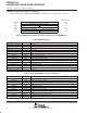
Table 2 shows the memory map address ranges of the device. Internal memory is always located at address
0 and can be used as both program and data memory. The configuration registers for the common peripherals
are located at the same hex address ranges. The external memory address ranges in the device begin at the
address location 0x8000 0000.
Table 2. TMS320C6711D Memory Map Summary
MEMORY BLOCK DESCRIPTION BLOCK SIZE (BYTES) HEX ADDRESS RANGE
Internal RAM (L2) 64K 0000 0000 – 0000 FFFF
Reserved 24M – 64K 0001 0000 – 017F FFFF
External Memory Interface (EMIF) Registers 256K 0180 0000 – 0183 FFFF
L2 Registers 256K 0184 0000 – 0187 FFFF
HPI Registers 256K 0188 0000 – 018B FFFF
McBSP 0 Registers 256K 018C 0000 – 018F FFFF
McBSP 1 Registers 256K 0190 0000 – 0193 FFFF
Timer 0 Registers 256K 0194 0000 – 0197 FFFF
Timer 1 Registers 256K 0198 0000 – 019B FFFF
Interrupt Selector Registers 512 019C 0000 – 019C 01FF
Device Configuration Registers 4 019C 0200 – 019C 0203
Reserved 256K − 516 019C 0204 – 019F FFFF
EDMA RAM and EDMA Registers 256K 01A0 0000 – 01A3 FFFF
Reserved 768K 01A4 0000 – 01AF FFFF
GPIO Registers 16K 01B0 0000 – 01B0 3FFF
Reserved 480K 01B0 4000 – 01B7 BFFF
PLL Controller Registers 8K 01B7 C000 – 01B7 DFFF
Reserved 4M + 520K 01B7 E000 – 01FF FFFF
QDMA Registers 52 0200 0000 – 0200 0033
Reserved 736M – 52 0200 0034 – 2FFF FFFF
McBSP 0 Data/Peripheral Data Bus 64M 3000 0000 – 33FF FFFF
McBSP 1 Data/Peripheral Data Bus 64M 3400 0000 – 37FF FFFF
Reserved 64M 3800 0000 – 3BFF FFFF
Reserved 1G + 64M 3C00 0000 – 7FFF FFFF
EMIF CE0
†
256M 8000 0000 – 8FFF FFFF
EMIF CE1
†
256M 9000 0000 – 9FFF FFFF
EMIF CE2
†
256M A000 0000 – AFFF FFFF
EMIF CE3
†
256M B000 0000 – BFFF FFFF
Reserved 1G C000 0000 – FFFF FFFF
†
The number of EMIF address pins (EA[21:2]) limits the maximum addressable memory (SDRAM) to 128MB per CE space. To get 256MB of
addressable memory, additional general-purpose output pin or external logic is required.