
- Texas Instruments Floating Point Digital Signal Processor Specification Sheet


SPRS292A − OCTOBER 2005 − REVISED NOVEMBER 2005
16
POST OFFICE BOX 1443 • HOUSTON, TEXAS 77251−1443
peripheral register descriptions (continued)
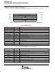
Table 13. Timer 0 and Timer 1 Registers
HEX ADDRESS RANGE
ACRONYM
REGISTER NAME
COMMENTS
TIMER 0 TIMER 1
ACRONYM
REGISTER NAME
COMMENTS
0194 0000 0198 0000 CTLx Timer x control register
Determines the operating
mode of the timer, monitors the
timer status, and controls the
function of the TOUT pin.
0194 0004 0198 0004 PRDx Timer x period register
Contains the number of timer
input clock cycles to count.
This number controls the
TSTAT signal frequency.
0194 0008 0198 0008 CNTx Timer x counter register
Contains the current value of
the incrementing counter.
0194 000C − 0197 FFFF 0198 000C − 019B FFFF − Reserved −
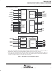
Table 14. McBSP0 and McBSP1 Registers
HEX ADDRESS RANGE
ACRONYM
REGISTER DESCRIPTION
McBSP0 McBSP1
ACRONYM
REGISTER DESCRIPTION
018C 0000 0190 0000 DRRx
McBSPx data receive register via Configuration Bus
The CPU and EDMA controller can only read this register;
they cannot write to it.
3000 0000 − 33FF FFFF 3400 0000 − 37FF FFFF DRRx McBSPx data receive register via Peripheral Data Bus
018C 0004 0190 0004 DXRx McBSPx data transmit register via Configuration Bus
3000 0000 − 33FF FFFF 3400 0000 − 37FF FFFF DXRx McBSPx data transmit register via Peripheral Data Bus
018C 0008 0190 0008 SPCRx McBSPx serial port control register
018C 000C 0190 000C RCRx McBSPx receive control register
018C 0010 0190 0010 XCRx McBSPx transmit control register
018C 0014 0190 0014 SRGRx McBSPx sample rate generator register
018C 0018 0190 0018 MCRx McBSPx multichannel control register
018C 001C 0190 001C RCERx McBSPx receive channel enable register
018C 0020 0190 0020 XCERx McBSPx transmit channel enable register
018C 0024 0190 0024 PCRx McBSPx pin control register
018C 0028 − 018F FFFF 0190 0028 − 0193 FFFF − Reserved