
- Texas Instruments Floating Point Digital Signal Processor Specification Sheet


SPRS292A − OCTOBER 2005 − REVISED NOVEMBER 2005
17
POST OFFICE BOX 1443 • HOUSTON, TEXAS 77251−1443
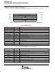
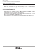
signal groups description
HHWIL
HCNTL0
HCNTL1
TRST
EXT_INT7
‡
IEEE Standard
1149.1
(JTAG)
Emulation
Reserved
Data
Register Select
Half-Word
Select
Reset and
Interrupts
Control
HPI
(Host-Port Interface)
16
Control/Status
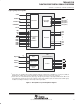
TDI
TDO
TMS
TCK
EMU0
EMU1
HD[15:0]
NMI
HAS
HR/W
HCS
HDS1
HDS2
HRDY
HINT
EXT_INT6
‡
EXT_INT5
‡
EXT_INT4
‡
RESET
RSV
RSV
RSV
RSV
RSV
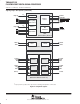
Clock/PLL
CLKIN
CLKOUT2
†
CLKMODE0
CLKOUT3
EMU2
EMU3
EMU4
EMU5
RSV
PLLHV
•
•
•
†
For this device, the CLKOUT2 pin is multiplexed with the GP[2] pin. Default function is CLKOUT2. To use this pin as GPIO, the
GP2EN bit in the GPEN register and the GP2DIR bit in the GPDIR register must be properly configured.
‡
For this device, the external interrupts (EXT_INT[7−4]) go through the general-purpose input/output (GPIO) module. When used
as interrupt inputs, the GP[7−4] pins must be configured as inputs (via the GPDIR register) and enabled (via the GPEN register)
in addition to enabling the interrupts in the interrupt enable register (IER).
Figure 3. CPU (DSP Core) and Peripheral Signals