
- Texas Instruments Floating Point Digital Signal Processor Specification Sheet

SPRS292A − OCTOBER 2005 − REVISED NOVEMBER 2005
2
POST OFFICE BOX 1443 • HOUSTON, TEXAS 77251−1443
Table of Contents
EMIF big endian mode correctness 60. . . . . . . . . . . . . . . .
bootmode 61. . . . . . . . . . . . . . . . . . . . . . . . . . . . . . . . . . . . . .
reset 61. . . . . . . . . . . . . . . . . . . . . . . . . . . . . . . . . . . . . . . . . . .
absolute maximum ratings over operating case
temperature range 62. . . . . . . . . . . . . . . . . . . . . . . . . .
recommended operating conditions 62. . . . . . . . . . . . . . . .
electrical characteristics over recommended ranges of
supply voltage and operating case temperature 63.
parameter measurement information 64. . . . . . . . . . . . . . .
signal transition levels 64. . . . . . . . . . . . . . . . . . . . . . . . . .
timing parameters and board routing analysis 66. . . . . .
input and output clocks 68. . . . . . . . . . . . . . . . . . . . . . . . . . .
asynchronous memory timing 71. . . . . . . . . . . . . . . . . . . . .
synchronous-burst memory timing 74. . . . . . . . . . . . . . . . .
synchronous DRAM timing 76. . . . . . . . . . . . . . . . . . . . . . . .
HOLD
/HOLDA timing 82. . . . . . . . . . . . . . . . . . . . . . . . . . . .
BUSREQ timing 83. . . . . . . . . . . . . . . . . . . . . . . . . . . . . . . . .
reset timing 84. . . . . . . . . . . . . . . . . . . . . . . . . . . . . . . . . . . . .
external interrupt timing 86. . . . . . . . . . . . . . . . . . . . . . . . . .
host-port interface timing 87. . . . . . . . . . . . . . . . . . . . . . . . .
multichannel buffered serial port timing 91. . . . . . . . . . . . .
timer timing 100. . . . . . . . . . . . . . . . . . . . . . . . . . . . . . . . . . . .
general-purpose input/output (GPIO) port timing 101. . . .
JTAG test-port timing 102. . . . . . . . . . . . . . . . . . . . . . . . . . .
mechanical data 103. . . . . . . . . . . . . . . . . . . . . . . . . . . . . . . .
revision history 3. . . . . . . . . . . . . . . . . . . . . . . . . . . . . . . . . . . . . .
GDP and ZDP BGA packages (bottom view) 4. . . . . . . . . . . .
description 5. . . . . . . . . . . . . . . . . . . . . . . . . . . . . . . . . . . . . . . . .
device characteristics 6. . . . . . . . . . . . . . . . . . . . . . . . . . . . . . . .
device compatibility 7. . . . . . . . . . . . . . . . . . . . . . . . . . . . . . . . . .
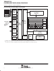
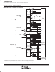
functional block and CPU (DSP core) diagram 8. . . . . . . . . . .
CPU (DSP core) description 9. . . . . . . . . . . . . . . . . . . . . . . . . .
memory map summary 11. . . . . . . . . . . . . . . . . . . . . . . . . . . . . .
peripheral register descriptions 12. . . . . . . . . . . . . . . . . . . . . . .
signal groups description 17. . . . . . . . . . . . . . . . . . . . . . . . . . . .
device configurations 20. . . . . . . . . . . . . . . . . . . . . . . . . . . . . . .
terminal functions 23. . . . . . . . . . . . . . . . . . . . . . . . . . . . . . . . . .
development support 36. . . . . . . . . . . . . . . . . . . . . . . . . . . . . . . .
device support 37. . . . . . . . . . . . . . . . . . . . . . . . . . . . . . . . . . . . .
CPU CSR register description 40. . . . . . . . . . . . . . . . . . . . . . . .
cache configuration (CCFG) register description 42. . . . . . . .
interrupt sources and interrupt selector 43. . . . . . . . . . . . . . . .
EDMA module and EDMA selector 44. . . . . . . . . . . . . . . . . . . .
PLL and PLL controller 46. . . . . . . . . . . . . . . . . . . . . . . . . . . . . .
general-purpose input/output (GPIO) 53. . . . . . . . . . . . . . . . . .
power-down mode logic 54. . . . . . . . . . . . . . . . . . . . . . . . . . . . .
power-supply sequencing 56. . . . . . . . . . . . . . . . . . . . . . . . . . . .
power-supply decoupling 58. . . . . . . . . . . . . . . . . . . . . . . . . . . .
IEEE 1149.1 JTAG compatibility statement 58. . . . . . . . . . . . .
EMIF device speed 59. . . . . . . . . . . . . . . . . . . . . . . . . . . . . . . . .