
- Texas Instruments Floating Point Digital Signal Processor Specification Sheet


SPRS292A − OCTOBER 2005 − REVISED NOVEMBER 2005
27
POST OFFICE BOX 1443 • HOUSTON, TEXAS 77251−1443
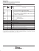
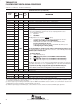
Terminal Functions (Continued)
SIGNAL
PIN
NO.
TYPE
†
IPD/
‡
DESCRIPTION
SIGNAL
NAME
GDP/
ZDP
TYPE
†
IPD/
IPU
‡
DESCRIPTION
EMIF − CONTROL SIGNALS COMMON TO ALL TYPES OF MEMORY
¶
(CONTINUED)
HRDY H19 O IPD Host ready (from DSP to host)
CE3 V6 O/Z IPU
Memory space enables
CE2 W6 O/Z IPU
Memory space enables
• Enabled by bits 28 through 31 of the word address
CE1 W18 O/Z IPU
•
Enabled by bits 28 through 31 of the word address
•
Only one asserted during any external data access
CE0 V17 O/Z IPU
• Only one asserted during any external data access
BE3 V5 O/Z IPU
Byte-enable control
BE2 Y4 O/Z IPU
Byte-enable control
•
Decoded from the two lowest bits of the internal address
BE1 U19 O/Z IPU
• Decoded from the two lowest bits of the internal address
• Byte-write enables for most types of memory
Can be directly connected to SDRAM read and write mask signal (SDQM)
BE0 V20 O/Z IPU
Byte-write enables for most types of memory
• Can be directly connected to SDRAM read and write mask signal (SDQM)
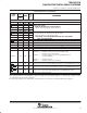
EMIF − BUS ARBITRATION
¶
HOLDA J18 O IPU Hold-request-acknowledge to the host
HOLD J17 I IPU Hold request from the host
BUSREQ J19 O IPU Bus request output
EMIF − ASYNCHRONOUS/SYNCHRONOUS MEMORY CONTROL
¶
ECLKIN Y11 I IPD External EMIF input clock source
ECLKOUT Y10 O/Z IPD
EMIF output clock depends on the EKSRC bit (DEVCFG.[4]) and on EKEN bit (GBLCTL.[5])
EKSRC = 0 – ECLKOUT is based on the internal SYSCLK3 signal
from the clock generator (default).
EKSRC = 1 – ECLKOUT is based on the the external EMIF input clock
source pin (ECLKIN)
EKEN = 0 – ECLKOUT held low
EKEN = 1 – ECLKOUT enabled to clock (default)
ARE/SDCAS/
SSADS
V11 O/Z IPU Asynchronous memory read enable/SDRAM column-address strobe/SBSRAM address strobe
AOE/SDRAS/
SSOE
W10 O/Z IPU Asynchronous memory output enable/SDRAM row-address strobe/SBSRAM output enable
AWE/SDWE/
SSWE
V12 O/Z IPU Asynchronous memory write enable/SDRAM write enable/SBSRAM write enable
ARDY Y5 I IPU Asynchronous memory ready input
†
I = Input, O = Output, Z = High impedance, S = Supply voltage, GND = Ground, A = Analog signal (PLL Filter)
‡
IPD = Internal pulldown, IPU = Internal pullup. [To oppose the supply rail on these IPD/IPU signal pins, use external pullup or pulldown resistors
no greater than 4.4 kΩ and 2.0 kΩ, respectively.]
¶
To maintain signal integrity for the EMIF signals, serial termination resistors should be inserted into all EMIF output signal lines.