
- Texas Instruments Floating Point Digital Signal Processor Specification Sheet

SPRS292A − OCTOBER 2005 − REVISED NOVEMBER 2005
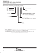
34
POST OFFICE BOX 1443 • HOUSTON, TEXAS 77251−1443
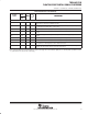
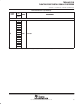
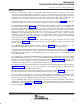
Terminal Functions (Continued)
SIGNAL
PIN
NO.
TYPE
†
DESCRIPTION
SIGNAL
NAME
GDP/
ZDP
TYPE
†
DESCRIPTION
GROUND PINS (CONTINUED)
D13
D17
E2
E4
E17
F19
G4
G17
H4
H17
J4
J9
J10
J11
J12
K2
K9
K10
Ground pins
#
V
SS
K11
GND
Ground pins
#
The center thermal balls (J9−J12, K9−K12, L9−L12, M9−M12) [shaded] are all tied to ground and act as
V
SS
K12
GND
The center thermal balls (J9−J12, K9−K12, L9−L12, M9−M12) [shaded] are all tied to ground and act as
both electrical grounds and thermal relief (thermal dissipation).
K20
both electrical grounds and thermal relief (thermal dissipation).
L9
L10
L11
L12
M4
M9
M10
M11
M12
M17
N4
N17
P4
P17
P19
T4
T17
†
I = Input, O = Output, Z = High impedance, S = Supply voltage, GND = Ground, A = Analog signal (PLL Filter)
#
Shaded pin numbers denote the center thermal balls for the GDP package.