
- Texas Instruments Floating Point Digital Signal Processor Specification Sheet

SPRS292A − OCTOBER 2005 − REVISED NOVEMBER 2005
62
POST OFFICE BOX 1443 • HOUSTON, TEXAS 77251−1443
absolute maximum ratings over operating case temperature range (unless otherwise noted)
†
Supply voltage range, CV
DD
(see Note 2) − 0.3 V to 1.8 V. . . . . . . . . . . . . . . . . . . . . . . . . . . . . . . . . . . . . . . . . .
Supply voltage range, DV
DD
(see Note 2) −0.3 V to 4 V. . . . . . . . . . . . . . . . . . . . . . . . . . . . . . . . . . . . . . . . . . . . .
Input voltage range −0.3 V to DV
DD
+ 0.5 V. . . . . . . . . . . . . . . . . . . . . . . . . . . . . . . . . . . . . . . . . . . . . . . . . . . .
Output voltage range −0.3 V to DV
DD
+ 0.5 V. . . . . . . . . . . . . . . . . . . . . . . . . . . . . . . . . . . . . . . . . . . . . . . . . . . .
Operating case temperature ranges, T
C
(default) 0_C to 90_C. . . . . . . . . . . . . . . . . . . . . . . . . . . . . . . . . .
(A version) [C6711DGDPA and C6711DZDPA] −40_C to105_C. . .
Storage temperature range, T
stg
−65_C to 150_C. . . . . . . . . . . . . . . . . . . . . . . . . . . . . . . . . . . . . . . . . . . . . . .
†
Stresses beyond those listed under “absolute maximum ratings” may cause permanent damage to the device. These are stress ratings only, and
functional operation of the device at these or any other conditions beyond those indicated under “recommended operating conditions” is not
implied. Exposure to absolute-maximum-rated conditions for extended periods may affect device reliability.
NOTE 2: All voltage values are with respect to V
SS
.
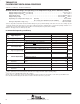
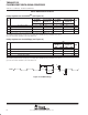
recommended operating conditions
‡
MIN NOM MAX UNIT
CV
DD
Supply voltage, Core
−250 only 1.33 1.4 1.47 V
CV
DD
Supply voltage, Core
1.14
§
1.20
§
1.32 V
DV
DD
Supply voltage, I/O 3.13 3.3 3.47 V
V
SS
Supply ground 0 0 0 V
V
IH
High-level input voltage
All signals except CLKS1, DR1, and RESET 2
V
V
IH
High-level input voltage
CLKS1, DR1, and RESET
2
V
V
IL
Low-level input voltage
All signals except CLKS1, DR1, and RESET 0.8
V
V
IL
Low-level input voltage
CLKS1, DR1, and RESET
0.3*DV
DD
V
I
OH
High-level output current
¶
All signals except ECLKOUT, CLKOUT2, CLKS1, and
DR1
–8
mA
I
OH
High-level output current
¶
ECLKOUT and CLKOUT2 –16
mA
I
OL
Low-level output current
¶
All signals except ECLKOUT, CLKOUT2, CLKS1, and
DR1
8 mA
I
OL
Low-level output current
¶
ECLKOUT and CLKOUT2 16 mA
CLKS1 and DR1 3 mA
T
C
Operating case
temperature
Default 0 90 _C
V
OS
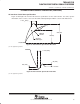
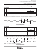
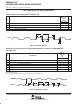
Maximum voltage during overshoot (See Figure 19) 4
#
V
V
US
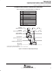
Maximum voltage during undershoot (See Figure 20) −0.7
#
V
T
C
Operating case
temperature
A version (C6711DGDPA and C6711DZDPA) –40 105 _C
‡
The core supply should be powered up prior to (and powered down after), the I/O supply. Systems should be designed to ensure that neither
supply is powered up for an extended period of time if the other supply is below the proper operating voltage.
§
These values are compatible with existing 1.26−V designs.
¶
Refers to DC (or steady state) currents only, actual switching currents are higher. For more details, see the device-specific IBIS models.
#
The absolute maximum ratings should not be exceeded for more than 30% of the cycle period.