
- Texas Instruments Floating Point Digital Signal Processor Specification Sheet

SPRS292A − OCTOBER 2005 − REVISED NOVEMBER 2005
64
POST OFFICE BOX 1443 • HOUSTON, TEXAS 77251−1443
PARAMETER MEASUREMENT INFORMATION
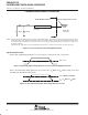
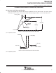
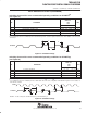
Transmission Line
4.0 pF 1.85 pF
Z0 = 50 Ω
(see note)
Tester Pin Electronics
Data Sheet Timing Reference Point
Output
Under
Test
NOTE: The data sheet provides timing at the device pin. For output timing analysis, the tester pin electronics and its transmission line effects
must be taken into account. A transmission line with a delay of 2 ns or longer can be used to produce the desired transmission line effect.
The transmission line is intended as a load only. It is not necessary to add or subtract the transmission line delay (2 ns or longer) from
the data sheet timings.
42 Ω 3.5 nH
Device Pin
(see note)
Input requirements in this data sheet are tested with an input slew rate of < 4 Volts per nanosecond (4 V/ns) at the device pin.
Figure 16. Test Load Circuit for AC Timing Measurements
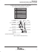
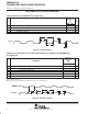
signal transition levels
All input and output timing parameters are referenced to 1.5 V for both “0” and “1” logic levels.
V
ref
= 1.5 V
Figure 17. Input and Output Voltage Reference Levels for AC Timing Measurements
All rise and fall transition timing parameters are referenced to V
IL
MAX and V
IH
MIN for input clocks, and
V
OL
MAX and V
OH
MIN for output clocks.
V
ref
= V
IL
MAX (or V
OL
MAX)
V
ref
= V
IH
MIN (or V
OH
MIN)
Figure 18. Rise and Fall Transition Time Voltage Reference Levels