
- Texas Instruments Floating Point Digital Signal Processor Specification Sheet

SPRS292A − OCTOBER 2005 − REVISED NOVEMBER 2005
68
POST OFFICE BOX 1443 • HOUSTON, TEXAS 77251−1443
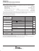
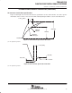
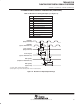
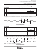
INPUT AND OUTPUT CLOCKS
timing requirements for CLKIN
†‡§
(see Figure 22)
GDPA-167, ZDPA−167 –200
NO
.
PLL MODE
(PLLEN = 1)
BYPASS MODE
(PLLEN = 0)
PLL MODE
(PLLEN = 1)
BYPASS MODE
(PLLEN = 0)
UNIT
MIN MAX MIN MAX MIN MAX MIN MAX
1 t
c(CLKIN)
Cycle time, CLKIN 6 83.3 6.7 5 83.3 6.7 ns
2 t
w(CLKINH)
Pulse duration, CLKIN high 0.4C 0.4C 0.4C 0.4C ns
3 t
w(CLKINL)
Pulse duration, CLKIN low 0.4C 0.4C 0.4C 0.4C ns
4 t
t(CLKIN)
Transition time, CLKIN 5 5 5 5 ns
†
The reference points for the rise and fall transitions are measured at V
IL
MAX and V
IH
MIN.
‡
C = CLKIN cycle time in nanoseconds (ns). For example, when CLKIN frequency is 40 MHz, use C = 25 ns.
§
See the PLL and PLL controller section of this data sheet.
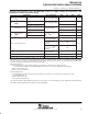
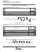
timing requirements for CLKIN
†‡§
(see Figure 22)
–250
NO
.
PLL MODE
(PLLEN = 1)
BYPASS MODE
(PLLEN = 0)
UNIT
MIN MAX MIN MAX
1 t
c(CLKIN)
Cycle time, CLKIN 4 83.3 6.7 ns
2 t
w(CLKINH)
Pulse duration, CLKIN high 0.4C 0.4C ns
3 t
w(CLKINL)
Pulse duration, CLKIN low 0.4C 0.4C ns
4 t
t(CLKIN)
Transition time, CLKIN 5 5 ns
†
The reference points for the rise and fall transitions are measured at V
IL
MAX and V
IH
MIN.
‡
C = CLKIN cycle time in nanoseconds (ns). For example, when CLKIN frequency is 40 MHz, use C = 25 ns.
§
See the PLL and PLL controller section of this data sheet.
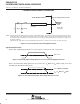
CLKIN
1
2
3
4
4
Figure 22. CLKIN Timings